

Communication mechanism
a communication mechanism and communication chip technology, applied in the field of communication devices, can solve the problems of increasing the number of wires, increasing delay, becoming impractical, etc., and achieve the effects of facilitating wire distribution around the chip, facilitating wire placement and routing, and increasing the distance of wires
- Summary
- Abstract
- Description
- Claims
- Application Information
AI Technical Summary
Benefits of technology
Problems solved by technology
Method used
Image

Examples
Embodiment Construction
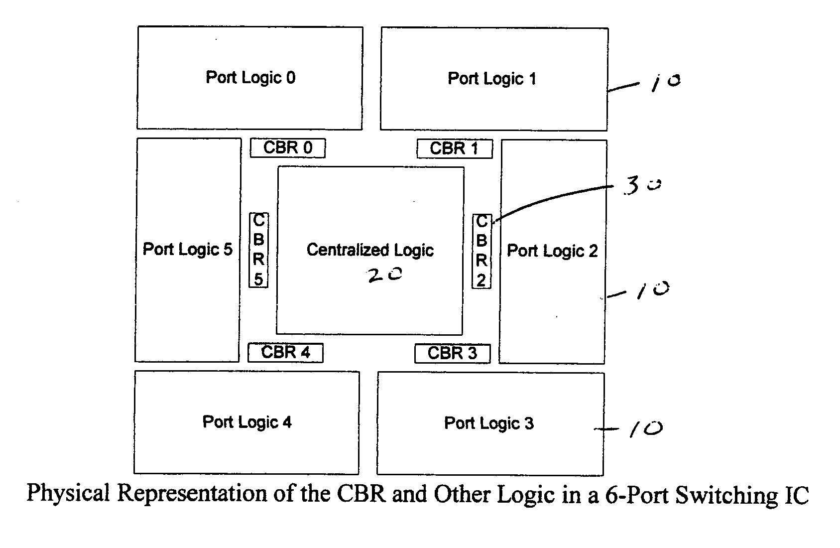
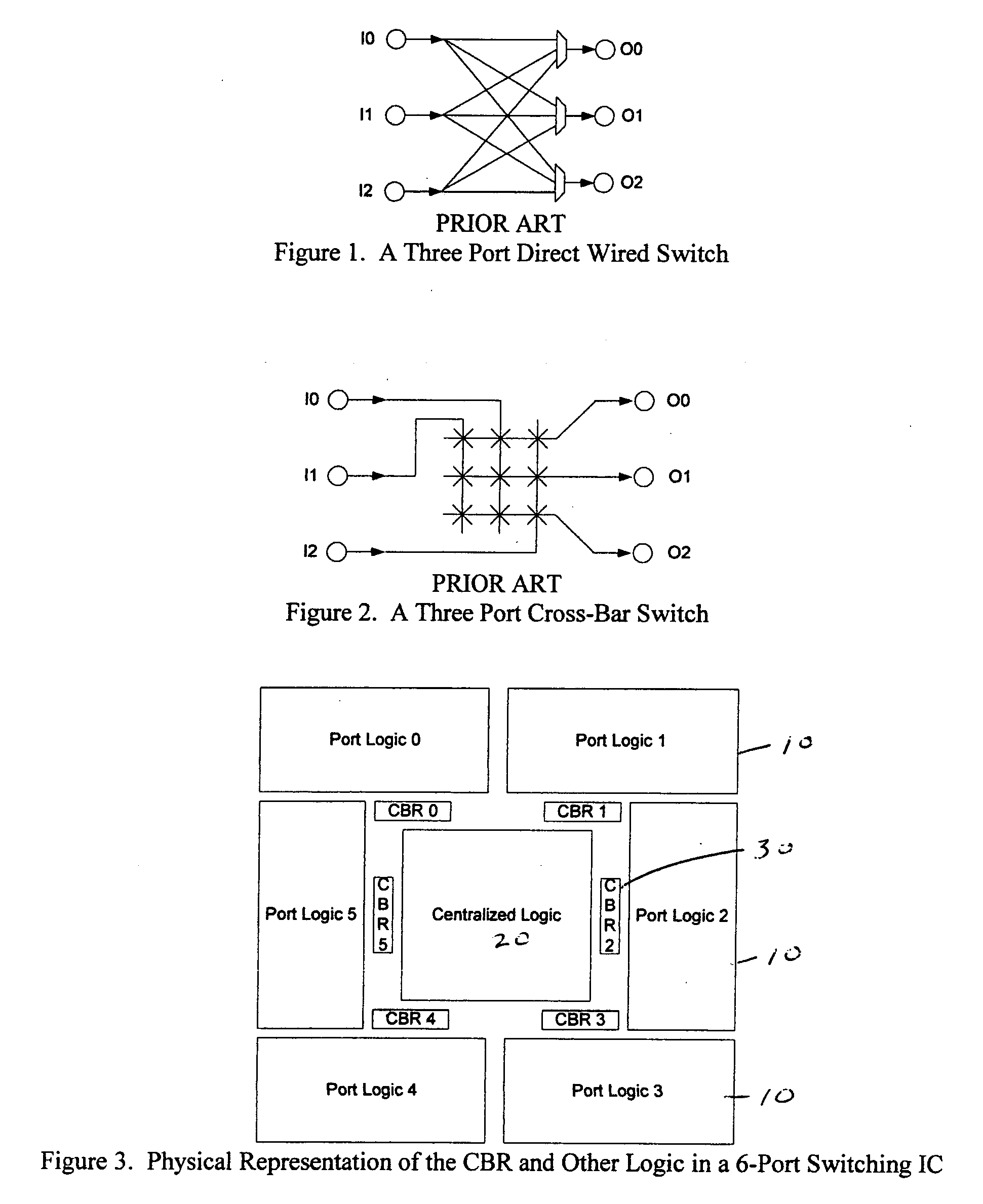
[0017] Switches are used to logically connect a set of input ports to a set of output ports. FIG. 3 shows a typical block diagram of a network switching device. This block diagram is also a physical layout or placement of the functional blocks within the device. Around the outer ring of the chip are 6 functional blocks 10, each associated with a particular input and output port. In the case of many switches, this port logic 10 is identical for each of the ports, although there is no requirement that this be the case. The port logic typically contains functions specifically associated with a particular port, such as transceivers, logic to determine a packet's port and class, FIFOs or buffers for incoming and outgoing packets. Physically located in the center of the IC is the centralized logic 20. Typically, this block 20 contains logic that allows the separate port logic blocks 10 to operate together as a single switch. Functions such as scheduling and centralized buffering, routing ...
PUM
 Abstract
Description
Claims
Application Information