Semiconductor device having polycide wiring layer, and manufacturing method of the same

a technology of silicide layer and semiconductor device, which is applied in the direction of semiconductor device, semiconductor/solid-state device details, electrical apparatus, etc., can solve the problems of increased rc delay, inability to control the thickness of the silicide layer with high precision, and inapplicable polycide wiring structur

Inactive Publication Date: 2006-04-13
KK TOSHIBA
View PDF7 Cites 9 Cited by
  • Summary
  • Abstract
  • Description
  • Claims
  • Application Information

AI Technical Summary

Problems solved by technology

The polycide wiring structure is not advantageously applied to devices requiring high-speed operations, because the polysilicon layer it uses has a higher resistance than that of a metal wiring layer (which is formed of Al or Cu) and therefore causes an increase in the RC delay.
However, the thickness of the silicide layer cannot be controlled with high precision when the layer is formed.
If the silicide layer is too thick, it may react with the gate insulating film and penetrate the gate insulating film, causing short circuits.

Method used


Image

  • Semiconductor device having polycide wiring layer, and manufacturing method of the same
  • Semiconductor device having polycide wiring layer, and manufacturing method of the same
  • Semiconductor device having polycide wiring layer, and manufacturing method of the same

Examples


first embodiment (

Trench-Type DRAM)

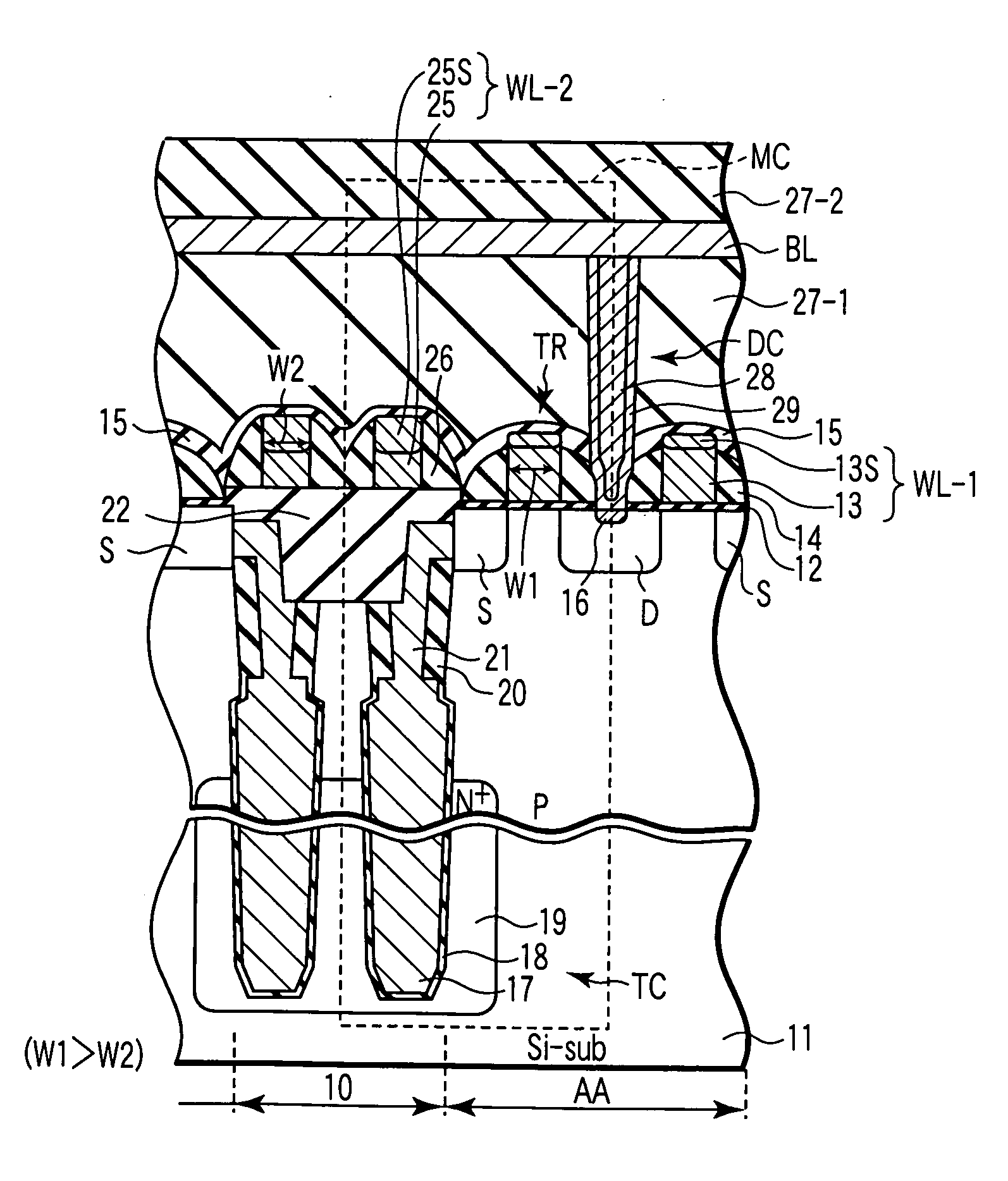
[0037] A semiconductor device according to the first embodiment of the present invention and a method for manufacturing the semiconductor device will now be described, referring to FIGS. 1 through 11. In the description of the first embodiment, the semiconductor device is a trench-type DRAM to which a polycide wiring structure is applied.

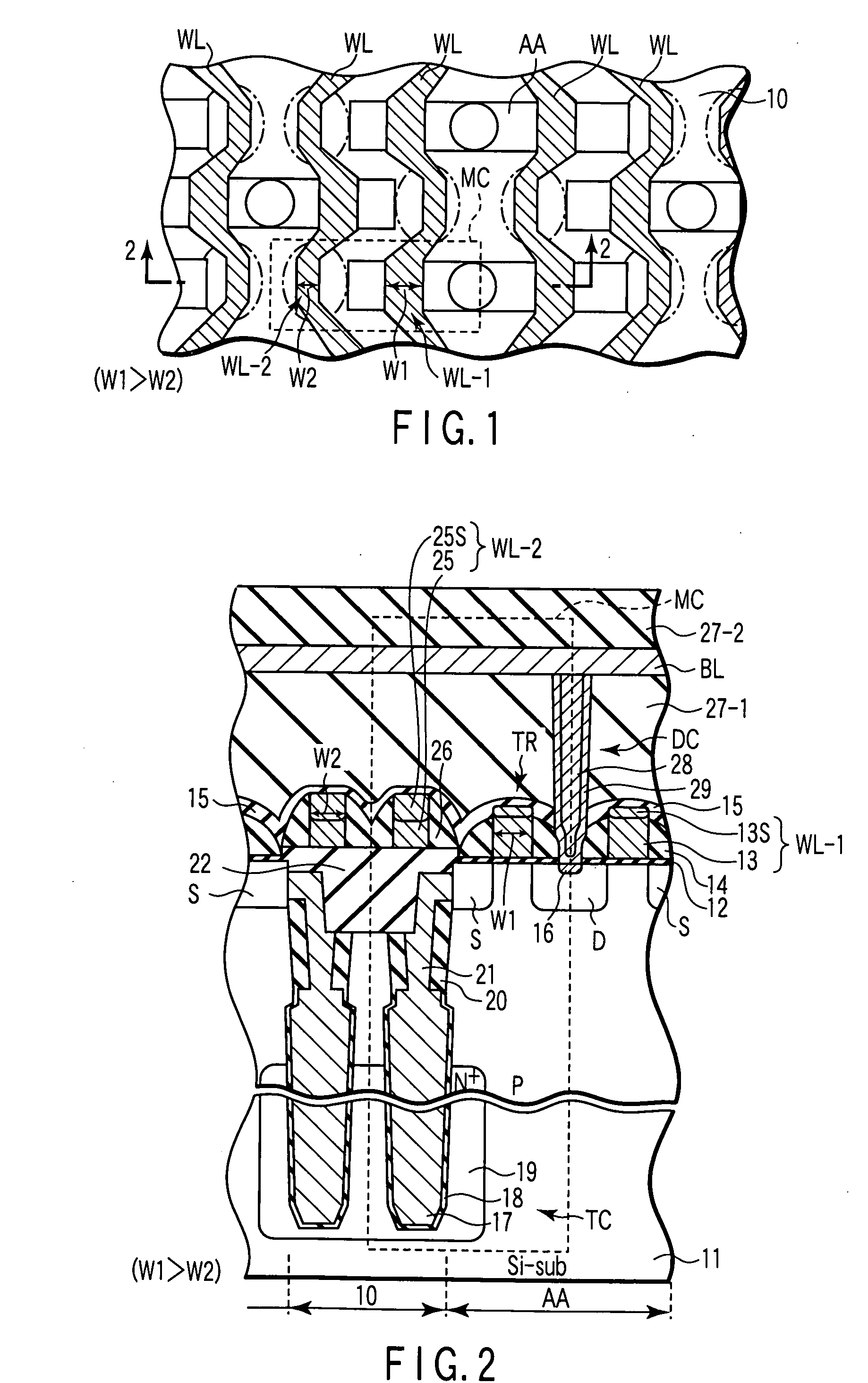
[0038]FIG. 1 is a plan view schematically illustrating a semiconductor device according to the first embodiment of the present invention. FIG. 2 is a sectional view taken along line 2-2 of FIG. 1.

[0039] Referring to FIGS. 1 and 2, an active area AA is formed on a P-type silicon substrate 11, and bit lines BL (not shown in FIG. 1) is provided in the active area AA. Word lines WL (conductive layers) are provided in such a manner that they extend in the direction crossing the bit lines BL. Trench-type DRAMs are provided at the intersections between the bit lines BL and the word lines WL. In FIGS. 1 and 2, the area indicated by the br...

second embodiment (

Trench-Type DRAM)

[0067] A semiconductor device according to the second embodiment of the present invention will now be described, referring to FIG. 9. In the descriptions below, structural elements similar to those of the first embodiment will not be mentioned for the sake of simplicity.

[0068]FIG. 9 is a sectional view taken in the same direction as FIG. 2.

[0069] As shown in FIG. 9, the spacer 26 and the shoulder portion 30 of silicide layer 25S are exposed more than the spacer 14 and the shoulder portion 31 of silicide layer 13S. In other words, spacer 26 is located higher than spacer 14.

[0070] The silicide layer 25S of the wiring layer WL-2 is thicker than the silicide layer 13S of the gate electrode WL-1. The silicide layer 25S of the semiconductor device of the second embodiment is thicker than the silicide layer 25S of the semiconductor device of the first embodiment.

[0071] As described above, in the semiconductor device of the second embodiment, the silicide layer 25S of t...

third embodiment (

Logic Circuit)

[0092] A semiconductor device according to the third embodiment of the present invention will now be described, referring to FIGS. 17 and 18. In the descriptions below, structural elements similar to those of the first and second embodiments will not be mentioned for the sake of simplicity. The third embodiment will be described, referring to a logic circuit having a polycide wiring structure.

[0093]FIG. 17 is a plan view schematically illustrating a semiconductor device according to the third embodiment of the present invention. FIG. 18 is a sectional view taken along line 18-18 of FIG. 17.

[0094] As shown in FIG. 18, transistors TR1 and TR2 are provided in an element region AA on the major surface of the semiconductor substrate 11. A wiring layer WL-2 is provided in an element isolation region 10, which is realized by shallow trench isolation (STI).

[0095] Transistor TR1 includes: a polysilicon layer 52 provided on a gate insulating film 51; a silicide layer 52S prov...


PUM


Abstract

A semiconductor device is provided with a semiconductor substrate comprising element isolation regions and an element region surrounded by the element isolation regions, a first polysilicon layer formed in the element region of the semiconductor substrate, an element-isolating insulation film formed in the element isolation region of the semiconductor substrate, a second polysilicon layer formed on the element-isolating insulation film, a first silicide layer formed on the first polysilicon layer. And the device further comprising a second silicide layer formed on the second polysilicon layer and being thicker than the first silicide layer.

Description

CROSS-REFERENCE TO RELATED APPLICATIONS [0001] This application is based upon and claims the benefit of priority from prior Japanese Patent Application No. 2004-272336, filed Sep. 17, 2004, the entire contents of which are incorporated herein by reference. BACKGROUND OF THE INVENTION [0002] 1. Field of the Invention [0003] The present invention relates to a semiconductor device having a polycide wiring structure, and also to a manufacturing method of the same. [0004] 2. Description of the Related Art [0005] A so-called polycide wiring structure is applied to many of the recent semiconductor devices since the structure is suited to high integration. In this polycide wiring structure, a polysilicon layer, which is the same layer as the gate electrode of a memory cell of a DRAM or a logic element, is extended continuously and used as a wiring layer. Compared to a metal wiring structure (wherein an allowance has to be provided between a contact and a gate, between different contacts, an...

Claims


Application Information

Patent Timeline
Patent Type & Authority Applications(United States)
IPC IPC(8): H01L29/94
CPCH01L21/76838H01L21/76889H01L23/53271H01L27/0207H01L27/10861H01L27/10891H01L2924/0002H01L27/10894H01L29/945H01L2924/00H10B12/038H10B12/488H10B12/09
Inventor MATSUDA, SATOSHI
Owner KK TOSHIBA
Why Eureka
Try Eureka