Transfer base substrate and method of semiconductor device

Active Publication Date: 2006-04-13
SAMSUNG ELECTRONICS CO LTD
View PDF4 Cites 17 Cited by
  • Summary
  • Abstract
  • Description
  • Claims
  • Application Information

AI Technical Summary

Benefits of technology

[0008] The advantage of the present invention is to provide a method of manufacturing a thin film semiconductor device, which can check defects of plurality of transfer thin film circuits formed on a transfer base substrate before transferring.
[0009] According to the first aspect of the invention, the transfer base substrate comprises; a substrate; a plurality of transfer thin film circuits formed on the substrate via removing layer, a test circuit formed on the substrate for checking circuit operation; and a wiring coupling each of transfer thin film circuits with a test circuit.
[0010] This structure can immediately check (test) defective or non-defective transfer thin film circuits which is an object of transfer before transferring since the transfer thin film circuits can be electrically coupled with a test circuit on a transfer base substrate. Further, it is possible to collect test data via computer system. Selecting non-defective transfer thin film circuits and using them can improve production yield of semiconductor devices as final products.
[0011] A plurality of transfer thin film circuits may be arranged in a

Problems solved by technology

There is no wiring for operating transfer thin film circuits on a transfer base substrate.
Namely, it is impossible to confirm the operation of transfer thin film circuits before transferring, even if some of malfunctioned transfer thin film circuits due to defects on manufacturing process on a transfer base substrate are existed.
Checking th

Method used


Image

  • Transfer base substrate and method of semiconductor device
  • Transfer base substrate and method of semiconductor device
  • Transfer base substrate and method of semiconductor device

Examples


first embodiment

[0036] Firstly, a technology of removing and transferring the above thin film semiconductor circuit is explained.

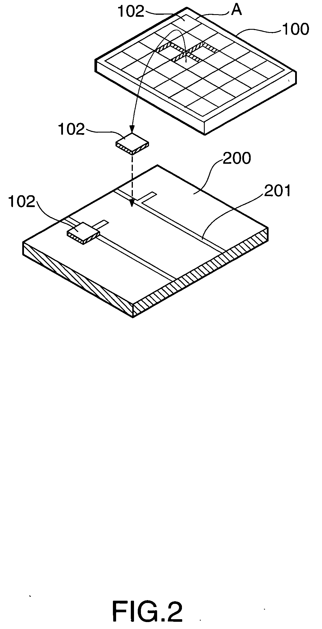
[0037]FIG. 2 is a schematic view of a method of removing and transferring. In this case, the substrate 100 is a transfer base substrate. As shown in the figure, a thin film circuits 102 is formed on the substrate 100 by a semiconductor process via removing layer (not shown.) The circuit becomes an object to be transferred. The film circuit 102 is formed in a plurality of regions A, which are arranged in a matrix on the substrate. As the above removing layer, an amorphous silicon layer is used.

[0038] Next, energy beam such as laser is irradiated onto a removing layer of thin film circuits 102 and destroys a part of the removing layer. Thin film circuits 102 are removed from a given part of the substrate 100 and placed on a predetermined position on a final substrate (a substrate receiving the transfer) 200. A wiring 201 is already formed on the substrate 200 and connecte...

second embodiment

[0045] In the second embodiment, wirings within the thin film circuits 102 in the above active matrix part 14a is used as wirings for test. The structure of the thin film circuits 102 and overall configuration are the same of the first embodiment and these explanations are omitted with referring them as the same reference numerals.

[0046]FIG. 8 is a enlarged view of the active matrix part 14a in the base transfer substrate 100 in the second embodiment. As shown in the figure, wirings Vsn, Data m for test go through an inner part of the thin film circuits 102. Many pads 104 are formed comparing with the first embodiment on each of the thin film circuits 102.

[0047] In the second embodiment, an area, which is assigned for a wiring connecting each of the thin film circuits 102, is small comparing with the first embodiment. Further, many areas can be assigned for the thin film circuits 102.

[0048]FIG. 9 is a cross sectional view of the active matrix part 14a in the base transfer substra...


PUM


Abstract

A transfer base substrate comprises: a substrate; a plurality of transfer thin film circuits formed on the substrate via removing layer; a test circuit formed on the substrate for checking circuit operation; and a wiring coupling each of transfer thin film circuits with a test circuit.

Description

RELATED APPLICATION INFORMATION [0001] This application claims priority to Japanese Application No. 2004-288080, filed Sep. 30, 2004. The contents of the Japanese Application are expressly incorporated herein by reference. BACKGROUND OF THE INVENTION [0002] 1. Technical Field [0003] The present invention is related to a semiconductor device and a method of testing a semiconductor device. More specifically, it is related to a transfer base substrate used for manufacturing a semiconductor device with remove and transfer technology of a thin film circuits and a method of testing a transfer base substrate. [0004] 2. Related Art [0005] It has been proposed that many of thin film elements or thin film circuits (transfer thin film circuits) having a given function, which is an object of transfer, are formed on a transfer base substrate by a semiconductor process and a part of formed transfer thin film circuits is transferred to a final substrate (a substrate, which receives transfer), manu...

Claims


Application Information

Patent Timeline
IPC IPC(8): H01L21/66
CPCG01R31/31715G01R31/31723G11C11/401G11C2029/0403G11C2029/5002H01L22/34H01L2924/0002H01L27/1214H01L27/1266H01L2924/00H01L27/12
Inventor HARA, HIROYUKISHIMODA, TATSUYA
Owner SAMSUNG ELECTRONICS CO LTD
Why Eureka
Try Eureka