

Coated semiconductor wafer, and process and apparatus for producing the semiconductor wafer
a technology of coating and semiconductor, applied in the direction of coating, chemically reactive gas, crystal growth process, etc., can solve the problem of more or less pronounced undesirable radial fluctuation in the resistivity of the epitaxial layer, transitions, likewise undesirable, etc., and achieve the effect of low nanotopology valu
- Summary
- Abstract
- Description
- Claims
- Application Information
AI Technical Summary
Benefits of technology
Problems solved by technology
Method used
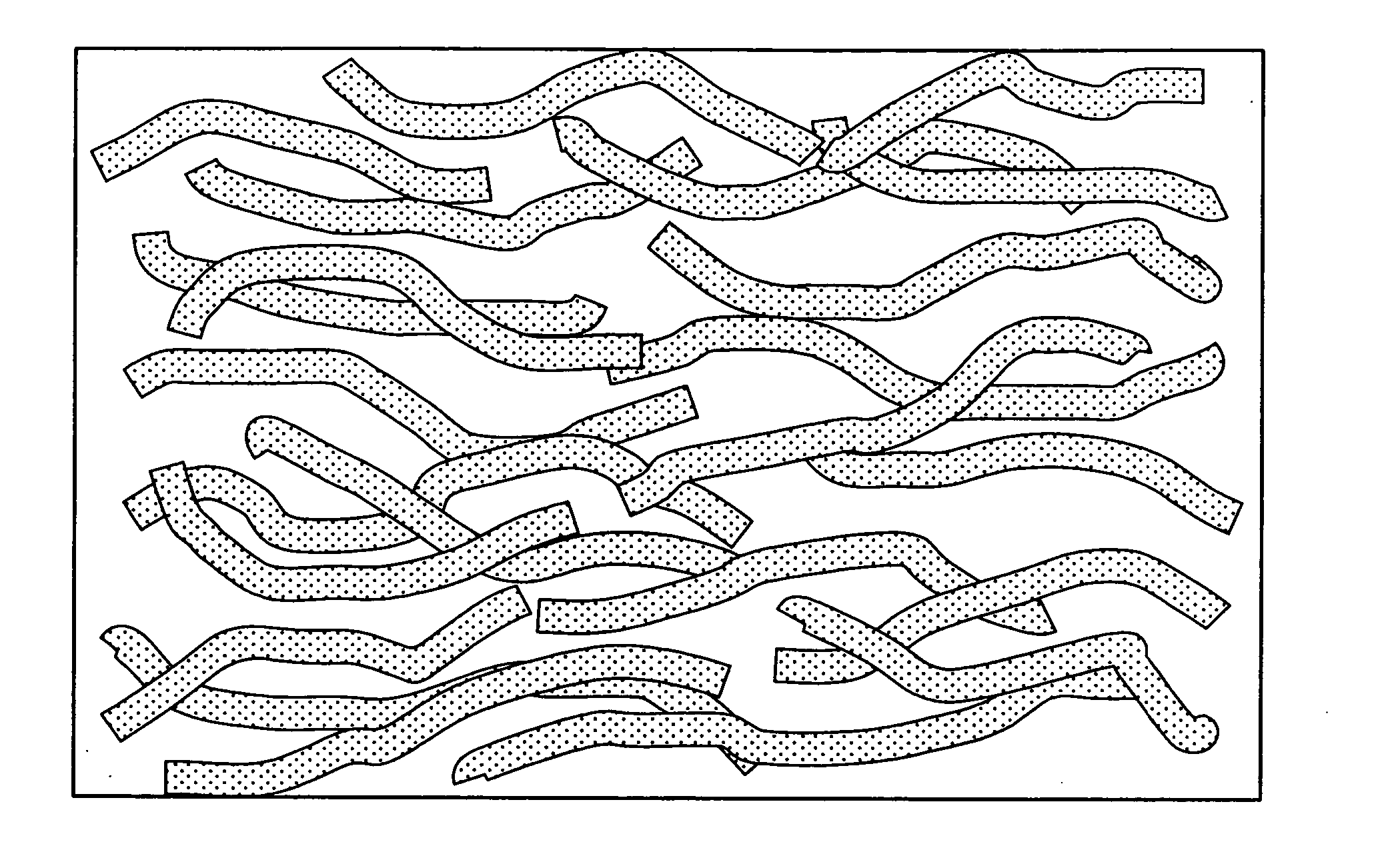
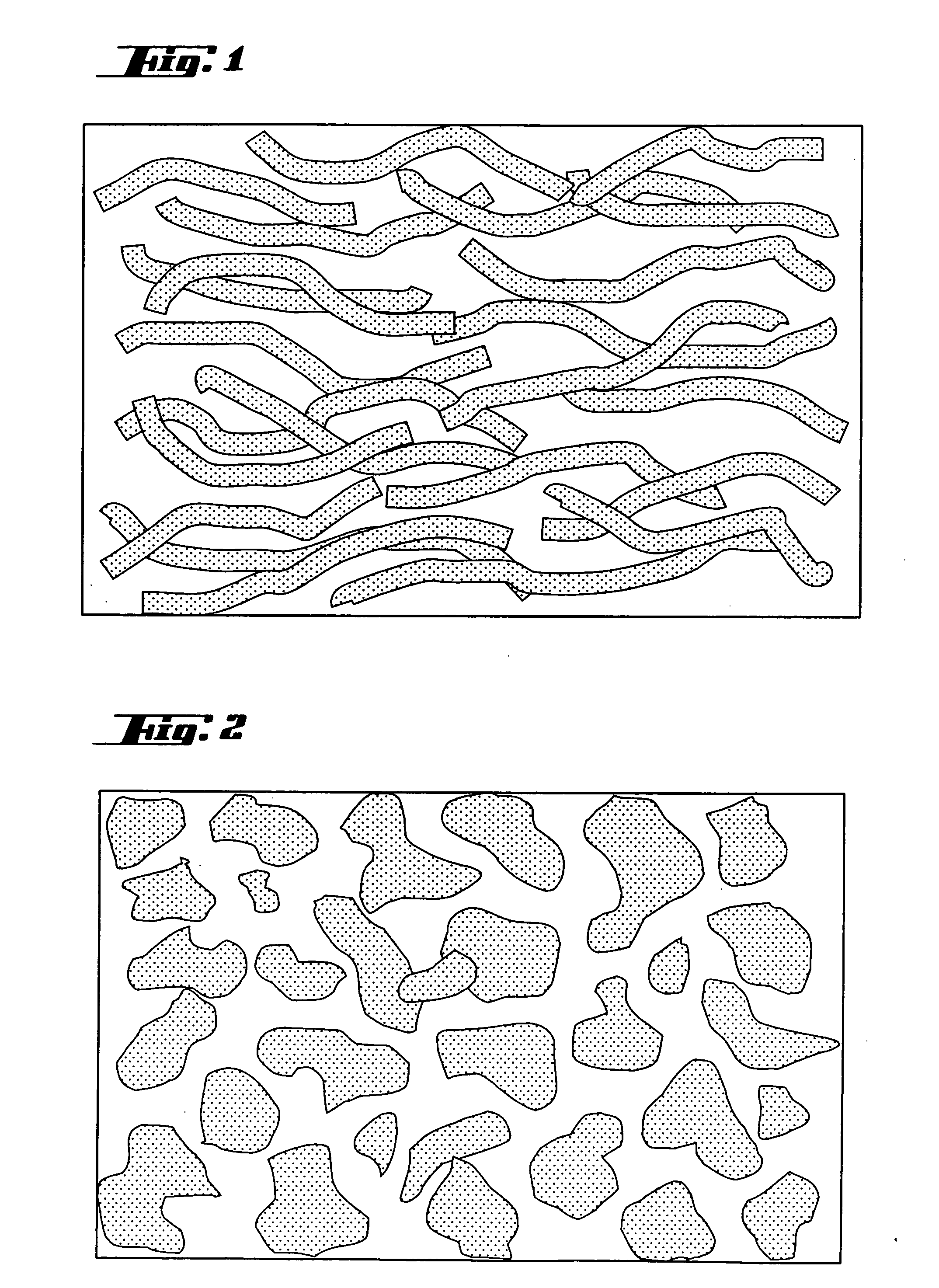
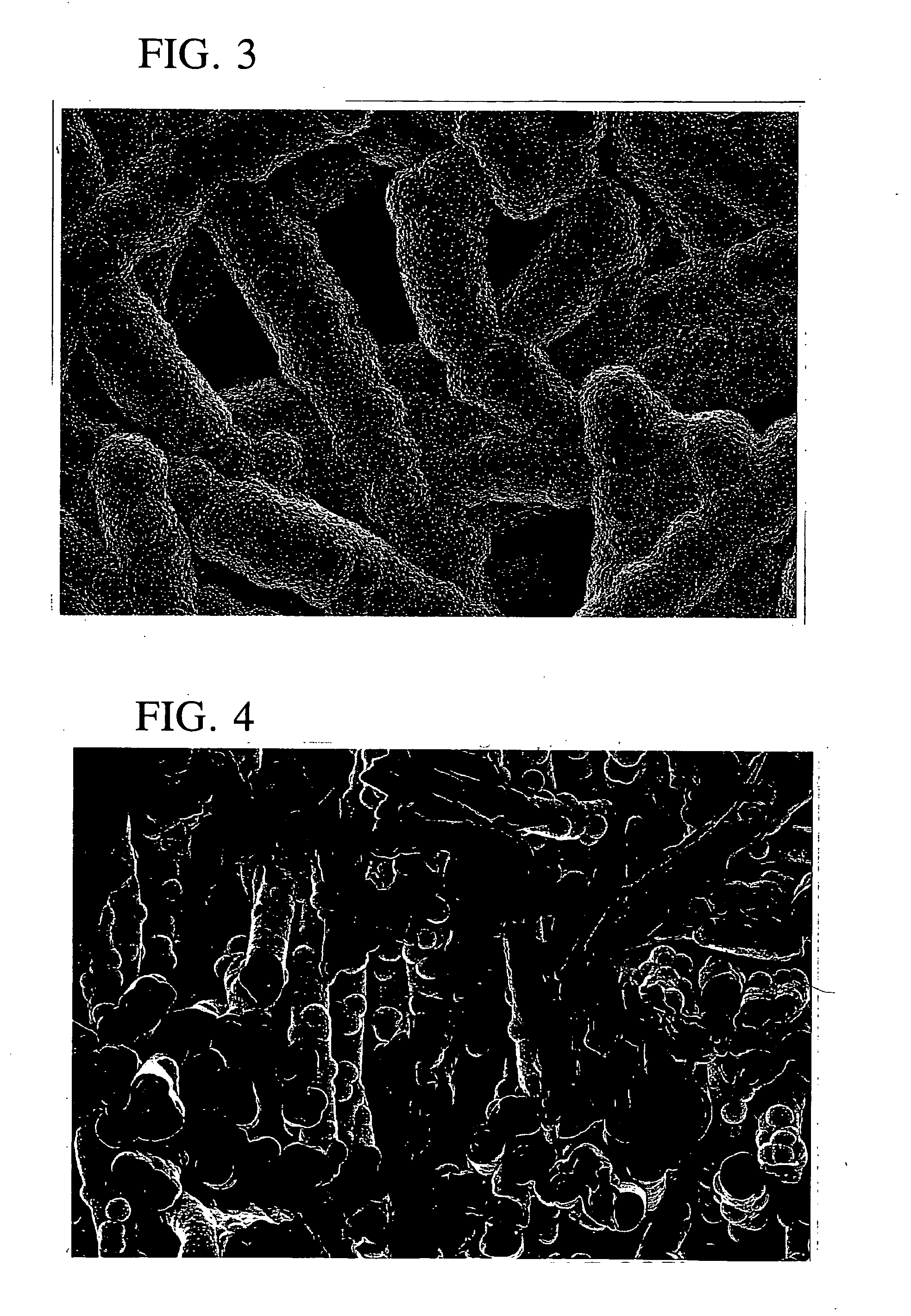
Image

Examples
Embodiment Construction
)
[0017] The subject matter of the invention is a semiconductor wafer having a front surface which has been coated by chemical vapor deposition (CVD) and a polished or etched back surface, wherein the nanotopography of the back surface, expressed as the PV (=peak to valley) height fluctuation, is less than 5 nm, and at the same time the halo of the back surface, expressed as haze, is less than 5 ppm.
[0018] The semiconductor wafer is preferably a silicon substrate wafer with an epitaxially deposited layer on the front surface. The back surface of the coated semiconductor wafer is polished or etched. The substrate wafer is preferably p-doped or n-doped, more preferably p-doped with boron as dopant, in which case the doping level may be p−, p, p+ and p++. A doping level p+, which corresponds to a resistivity of approximately 0.005 to approximately 0.03 ohm·cm, is particularly preferred. The epitaxial layer is preferably likewise p-doped, most preferably with boron as dopant, and prefer...
PUM
| Property | Measurement | Unit |
|---|---|---|
| pore diameter | aaaaa | aaaaa |
| density | aaaaa | aaaaa |
| porosity | aaaaa | aaaaa |
Abstract
Description
Claims
Application Information