Planar substrate devices integrated with finfets and method of manufacture

a technology of planar substrate and finfet, which is applied in the direction of semiconductor devices, electrical equipment, transistors, etc., can solve the problems of large height differences between finfet gates and gates, and increase the overall manufacturing cos

Active Publication Date: 2006-04-20
GLOBALFOUNDRIES U S INC
View PDF7 Cites 50 Cited by
  • Summary
  • Abstract
  • Description
  • Claims
  • Application Information

AI Technical Summary

Benefits of technology

[0011] The embodiments of the invention provide an easy to implement integration technique whereby the planar logic integrated circuit devices are incorporated with the FinFET devices and are formed such that the FET gate and FinFET gate are formed in one manufacturing step. For example, the deposition of the FET gate material and FinFET gate material occur at the same time, and the planarization of the FET gate material and FinFET gate material occur at the same time. The FET gate and FinFET gate are planarized to the same upper height, which obviates the need for additional lithography and etching processes, thereby reducing the number of manufacturing steps resulting in an overall reduction in manufacturing cost.

Problems solved by technology

However, this generally tends to result in large height differences between the FinFET gates and the gates over the planar logic (i.e., the FET gates).
As such, this step height difference is a significant problem for lithography and etching and requires several additional manufacturing steps to ameliorate the problem, which tends to increase the overall manufacturing cost.

Method used


Image

  • Planar substrate devices integrated with finfets and method of manufacture
  • Planar substrate devices integrated with finfets and method of manufacture
  • Planar substrate devices integrated with finfets and method of manufacture

Examples


Embodiment Construction

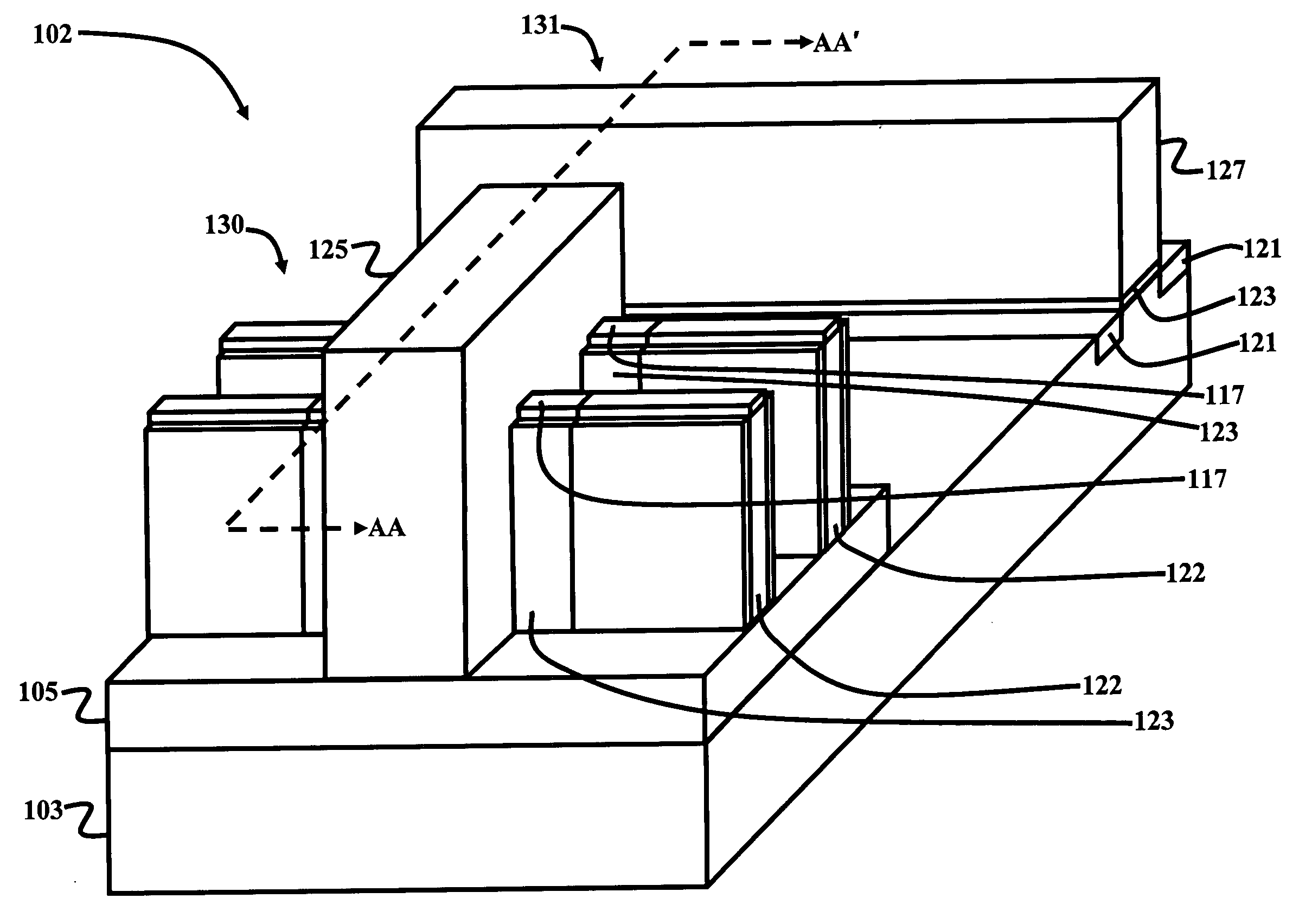
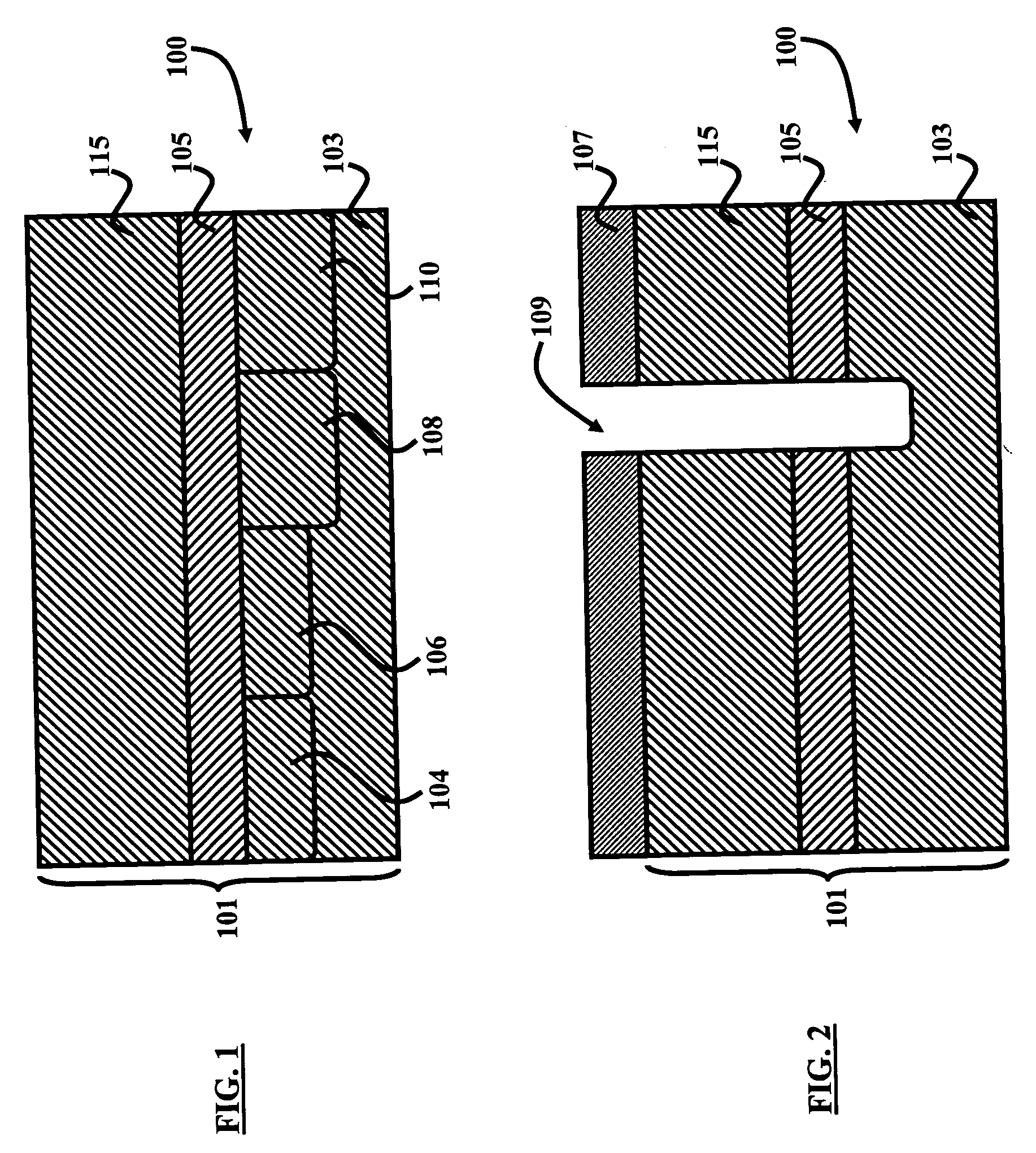
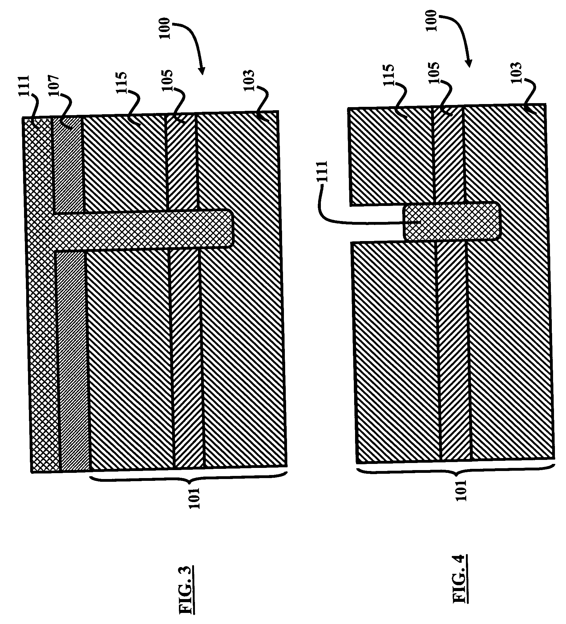
[0026] The embodiments of the invention and the various features and advantageous details thereof are explained more fully with reference to the non-limiting embodiments that are illustrated in the accompanying drawings and detailed in the following description. It should be noted that the features illustrated in the drawings are not necessarily drawn to scale. Descriptions of well-known components and processing techniques are omitted so as to not unnecessarily obscure the embodiments of the invention. The examples used herein are intended merely to facilitate an understanding of ways in which the embodiments of the invention may be practiced and to further enable those of skill in the art to practice the embodiments of the invention. Accordingly, the examples should not be construed as limiting the scope of the embodiments of the invention.

[0027] As mentioned, there remains a need for a novel method and structure, which provides superior IC device performance while simultaneously...


PUM


Abstract

A planar substrate device integrated with fin field effect transistors (FinFETs) and a method of manufacture comprises a silicon-on-insulator (SOI) wafer comprising a substrate; a buried insulator layer over the substrate; and a semiconductor layer over the buried insulator layer. The structure further comprises a FinFET over the buried insulator layer and a field effect transistor (FET) integrated in the substrate, wherein the FET gate is planar to the FinFET gate. The structure further comprises retrograde well regions configured in the substrate. In one embodiment, the structure further comprises a shallow trench isolation region configured in the substrate.

Description

CROSS-REFERENCE TO RELATED APPLICATIONS [0001] This Application is a division of U.S. patent application Ser. No. 10 / 711,974, filed Oct. 18, 2004, hereby incorporated by reference.BACKGROUND OF THE INVENTION [0002] 1. Field of the Invention [0003] The embodiments of the invention generally relate to microelectronic logic devices and methods of fabrication and more particularly to the design and manufacturing of integrated circuit devices having improved device performance characteristics and improved manufacturing methods. [0004] 2. Description of the Related Art [0005] As integrated circuits (ICs) continue to develop and enhance, the number and density of the devices being formed on IC substrates has increased tremendously with the fabrication of ICs having hundreds of millions and approaching billions of devices on a chip being standard in the industry. In conjunction with this increase in the number of devices formed on an IC substrate and the concurrent increase in density of th...

Claims


Application Information

Patent Timeline
Patent Type & Authority Applications(United States)
IPC IPC(8): H01L21/8234H01L21/336H01L21/8238H01L21/84H01L27/12H01L29/04H01L29/786
CPCH01L21/823821H01L21/823828H01L21/823878H01L21/845H01L27/1211H01L29/66795H01L29/785H01L27/0924
Inventor ANDERSON, BRENT A.NOWAK, EDWARD J.RANKIN, JED H.
Owner GLOBALFOUNDRIES U S INC
Why Eureka
Try Eureka