Semiconductor device

a semiconductor device and semiconductor technology, applied in semiconductor devices, digital storage, instruments, etc., can solve the problems of complex manufacturing process, increased manufacturing cost, reduced etc., to achieve the effect of reducing the number of manufacturing steps of semiconductor devices, increasing the manufacturing yield of semiconductor devices, and reducing the manufacturing cost of semiconductor devices

Active Publication Date: 2011-04-07
SEMICON ENERGY LAB CO LTD
View PDF16 Cites 44 Cited by
  • Summary
  • Abstract
  • Description
  • Claims
  • Application Information

AI Technical Summary

Benefits of technology

[0011]In the above-described semiconductor device, various elements such as a switching element, a capacitor, and a resistor are provided in addition to the memory element. Therefore, in order to manufacture the semiconductor device, many steps are required and the manufacturing process becomes complicated. As a result, the manufacturing yield of the semiconductor devices is decreased or a manufacturing cost is increased.
[0013]In view of the above problems, an object of one embodiment of the present invention is to improve the manufacturing yield of semiconductor devices.
[0014]Further, an object of one embodiment of the present invention is to reduce a manufacturing cost of a semiconductor device.
[0015]Furthermore, an object of one embodiment of the present invention is to reduce the area of an integrated circuit included in a semiconductor device.
[0023]A memory layer of a memory element and a resistive layer of a resistor are formed of the same material in a semiconductor device according to one embodiment of the present invention. Therefore, the memory layer and the resistive layer can be formed in the same step, whereby the number of manufacturing steps of the semiconductor device can be reduced. As a result, the manufacturing yield of the semiconductor devices can be increased or the manufacturing cost of the semiconductor device can be reduced.
[0024]In addition, the semiconductor device according to one embodiment of the present invention has a resistor including a resistive layer having high resistance value. Therefore, the area of an integrated circuit included in the semiconductor device can be reduced.

Problems solved by technology

Therefore, in order to manufacture the semiconductor device, many steps are required and the manufacturing process becomes complicated.
As a result, the manufacturing yield of the semiconductor devices is decreased or a manufacturing cost is increased.
When the resolution of the integrated circuit is increased, influence of parasitic capacitance between wirings or the like becomes apparent, whereby the area of the integrated circuit cannot be easily decreased.

Method used


Image

  • Semiconductor device
  • Semiconductor device
  • Semiconductor device

Examples


embodiment 1

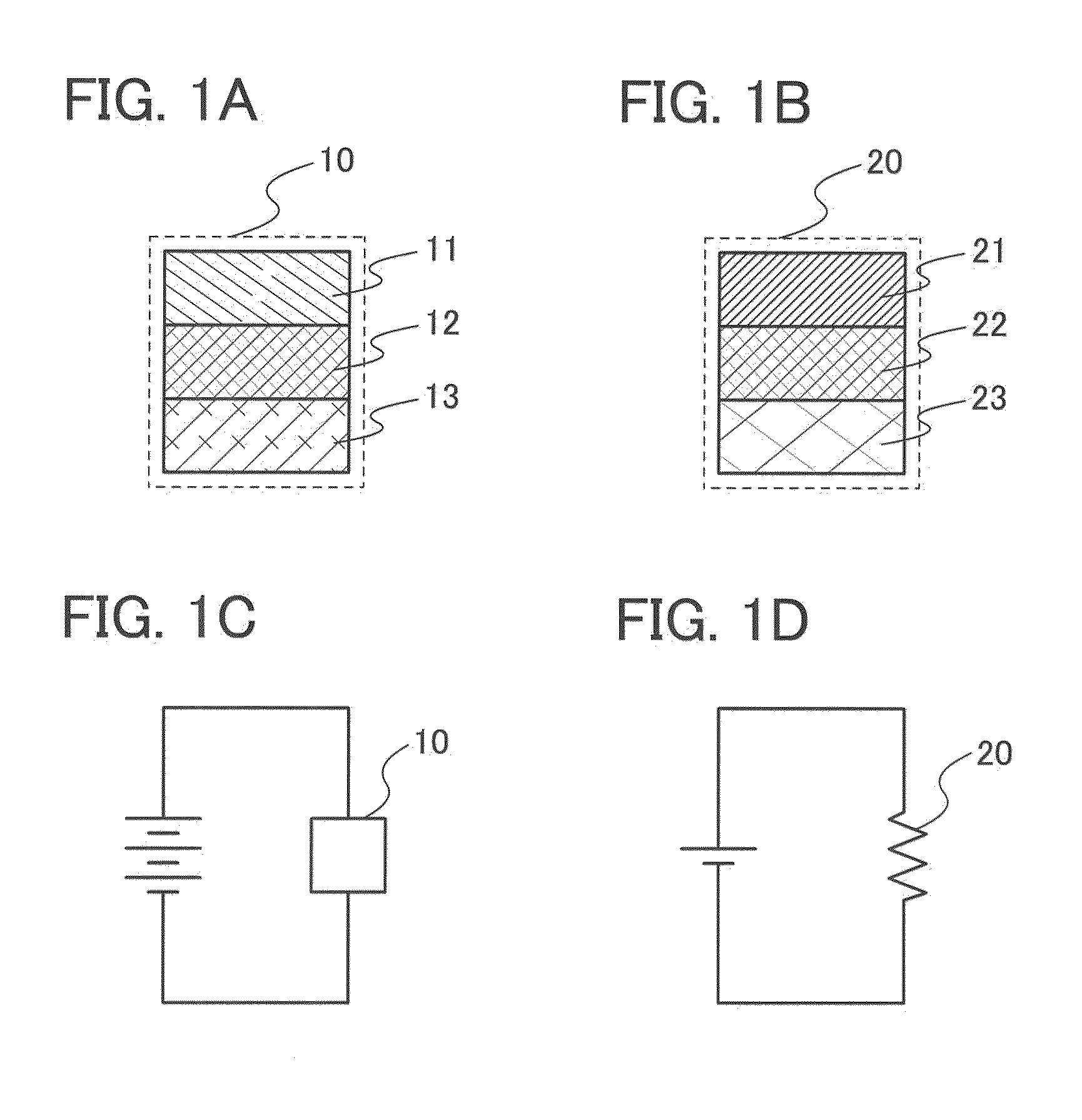
[0048]In this embodiment, an example of a semiconductor device including a memory element and a resistor is described with reference to FIGS. 1A to 1D.

[0049]FIG. 1A and FIG. 1B show a memory element 10 and a resistor 20 respectively, which are included in the semiconductor device of this embodiment. The memory element 10 shown in FIG. 1A includes a conductive layer 13, a memory layer 12 over the conductive layer 13, and a conductive layer 11 over the memory layer 12. The resistor 20 shown in FIG. 1B includes a conductive layer 23, a resistive layer 22 over the conductive layer 23, and a conductive layer 21 over the resistive layer 22. Note that the memory layer 12 and the resistive layer 22 are formed of the same material. In addition, the memory element 10 has a function of electrically connecting the conductive layer 11 and the conductive layer 13 by an irreversible reaction which is caused by dielectric breakdown of the memory layer 12 due to application of a voltage higher than ...

embodiment 2

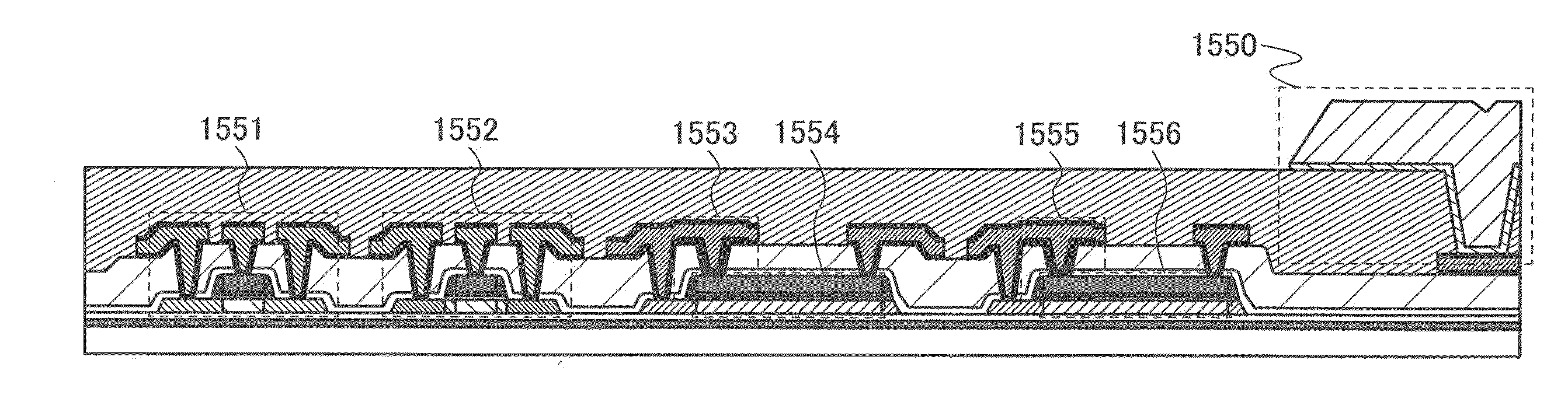
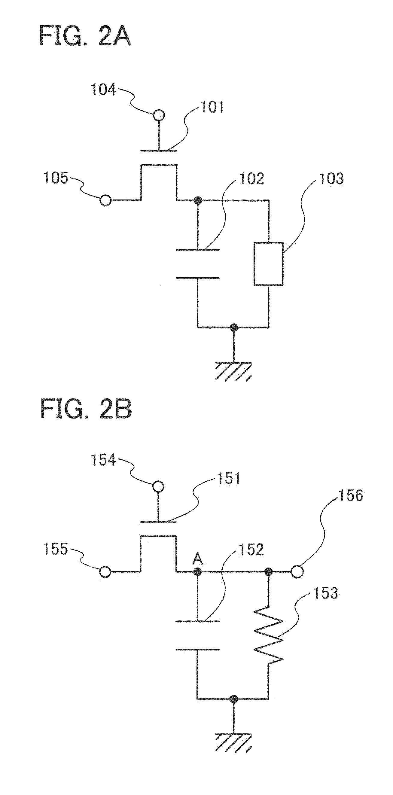
[0054]In this embodiment, examples of a semiconductor device in which a memory element and a resistor are formed over the same substrate and a manufacturing method thereof are described with reference to FIGS. 2A and 2B, FIGS. 3A and 3B, FIGS. 4A and 4B, FIGS. 5A to 5C, and FIGS. 6A to 6C. Specifically, a semiconductor device including a memory circuit and a flag circuit, which prevents an interrogator from reading the same information twice, is described.

[0055]FIG. 2A shows an example of a circuit configuration of the memory circuit included in the semiconductor of this embodiment. The memory circuit shown in FIG. 2A includes a transistor 101, a capacitor 102, and a memory element 103. In addition, a gate electrode and a first electrode of the transistor 101 are electrically connected to a control terminal 104 and an input-output terminal 105 respectively. One electrode of the capacitor 102 is electrically connected to a second electrode of the transistor 101 and the other thereof ...

embodiment 3

[0088]In this embodiment, an example of a semiconductor device having a memory element and a resistor is described with reference to FIG. 7. Specifically, a semiconductor device having a memory circuit and a reading circuit performing reading of information from the memory circuit is described.

[0089]FIG. 7 shows an example of a circuit configuration of a memory circuit and a reading circuit included in a semiconductor device of this embodiment.

[0090]A memory circuit 700 shown in FIG. 7 includes a transistor 701 and a memory element 702. Further, a gate electrode of the transistor 701 is electrically connected to a control terminal 703. One electrode of the memory element 702 is electrically connected to one electrode of the transistor 701, and the other thereof is grounded.

[0091]A reading circuit 750 shown in FIG. 7 has transistors 751 and 752, resistors 753 and 754, and a comparator 755. Further, a gate electrode of the transistor 751 is grounded. A first electrode of the transisto...


PUM


Abstract

Objects of the present invention are to improve the manufacturing yield of semiconductor devices, reduce manufacturing cost of the semiconductor device, and reduce the circuit area of an integrated circuit included in the semiconductor device. A memory layer of a memory element and a resistive layer of a resistor included in the semiconductor device are formed of the same material. Therefore, the memory layer and the resistive layer are formed in the same step, whereby the number of manufacturing steps of the semiconductor device can be reduced. As a result, the manufacturing yield of the semiconductor devices can be improved and the manufacturing cost can be reduced. In addition, the semiconductor device includes a resistor having a resistive component which has high resistance value. Consequently, the area of the integrated circuit included in the semiconductor device can be reduced.

Description

BACKGROUND OF THE INVENTION[0001]1. Field of the Invention[0002]The present invention relates to a semiconductor device. In particular, the present invention relates to a semiconductor device having a wireless communication function.[0003]Note that a semiconductor device in this specification refers to as a general device which can function by utilizing semiconductor characteristics, and electro-optical devices, semiconductor circuits, and electronic appliances are all semiconductor devices.[0004]2. Description of the Related Art[0005]Semiconductor devices having a wireless communication function for transmitting and receiving data wirelessly have been put into practical use in a variety of fields. Semiconductor devices having a wireless communication function is expected to further expand the market as a new mode of communication information terminals. In semiconductor devices having a wireless communication function, which are put into practical use, antennas and integrated circui...

Claims


Application Information

Patent Timeline
Patent Type & Authority Applications(United States)
IPC IPC(8): G11C11/56H01L45/00
CPCG11C13/004G11C17/16H01L27/24G11C2213/34G11C2213/79G11C2213/33H10B63/00
Inventor SAITO, TOSHIHIKOMATSUZAKI, TAKANORI
Owner SEMICON ENERGY LAB CO LTD
Why Eureka
Try Eureka