Reference current source for current sense amplifier and programmable resistor configured with magnetic tunnel junction cells

a current sense amplifier and programmable resistor technology, applied in the direction of information storage, static storage, digital storage, etc., can solve the problems of inability to reliably determine the programmed state of a memory device, inherent reliability and yield issues, and associated tight design margins, so as to improve the performance and reliability of reading information stored in a memory device

Inactive Publication Date: 2006-05-04
INFINEON TECH AG
View PDF6 Cites 159 Cited by
  • Summary
  • Abstract
  • Description
  • Claims
  • Application Information

AI Technical Summary

Benefits of technology

[0022] In one aspect, the present invention relates to the need to provide a memory device with high reliability and that is tolerant of ordinary manufacturing process variations without compromising device design margins. The present invention further relates to providing a memory device employing magnetic memory technology. Preferably, the present invention relates to magnetic memory technology in which the resistance of a memory device that is programmed to store a “0” (“unprogrammed”) and the resistance of a device that is programmed to store a “1” (“programmed”) does not change by more than a factor of two. The present invention further relates to providing an MRAM memory device employing MTJs. In a further aspect, the present invention relates to the utilization of the resistance characteristics of MTJ devices, including devices based on GMR or another mechanism in which a resistance is dependent on the direction of polarization of a free magnetic layer with respect to a fixed magnetic layer, that can exhibit at least two resistance values dependent on the magnetization polarity of two magnetic layers, and that can be coupled in arrays to increase device reliability or to provide fine adjustment of a circuit resistance. The present invention further relates to providing sufficiently redundant circuit elements that can source a reference cell current whereby a failure of one or more circuit elements does not result in a memory device failure. Co-pending U.S. patent application Ser. No. 10 / 326,367 (Attorney Docket 2002 P 50075 US), which is incorporated herein by reference as if included in its entirety, is directed towards an MRAM memory device employing one or two reference cells to source an average reference current for sensing the unknown programming state of an MRAM memory cell. In response, the preferred embodiment provides more accurate current-sourcing capability, tolerates individual component failures or parameter drift, and substantially desensitizes device performance to process variations such as due to manufacturing tolerances or operating temperature. Thereby the design and efficient manufacture of reliable and low cost MTJ memory devices is enabled.
[0028] Another embodiment of the present invention is a method of sourcing a reference current by employing a large number of memory cells, each memory cell conducting a current depending on its programmed state, summing the individual memory cell currents, and scaling the summed current to a required current level to produce an average current positioned midway between the current of a MTJ memory cell programmed to store a logic 0 and a memory cell programmed to store a logic 1. Preferably, more than four cells are employed to provide a reliable source for the reference current. The method preferably includes scaling the summed current with a current mirror, and preferably, the method includes configuring the memory cells with MTJs.
[0034] Embodiments of the present invention achieve technical advantages as a reference current source including a memory device including the reference current source. Advantages of embodiments of the present invention include increased performance and reliability in reading information stored in a memory device.

Problems solved by technology

A limiting factor often preventing the reliable determination of the programmed state of a memory device is the accuracy of a reference current source coupled to a current comparator in the memory cell state sensing circuit.
The extremely small feature sizes that are required and their distribution over the area of the die introduce inherent reliability and yield issues and the associated tight design margins that must be considered.
Prior art approaches using a small number of cells such as two or four cells do not provide circuit margins tolerant of a single cell failure or parameter drift.

Method used


Image

  • Reference current source for current sense amplifier and programmable resistor configured with magnetic tunnel junction cells
  • Reference current source for current sense amplifier and programmable resistor configured with magnetic tunnel junction cells
  • Reference current source for current sense amplifier and programmable resistor configured with magnetic tunnel junction cells

Examples


Embodiment Construction

[0049] The making and using of the presently preferred embodiments are discussed in detail below. It should be appreciated, however, that the present invention provides many applicable inventive concepts that can be embodied in a wide variety of specific contexts. The specific embodiments discussed are merely illustrative of specific ways to make and use the invention, and do not limit the scope of the invention.

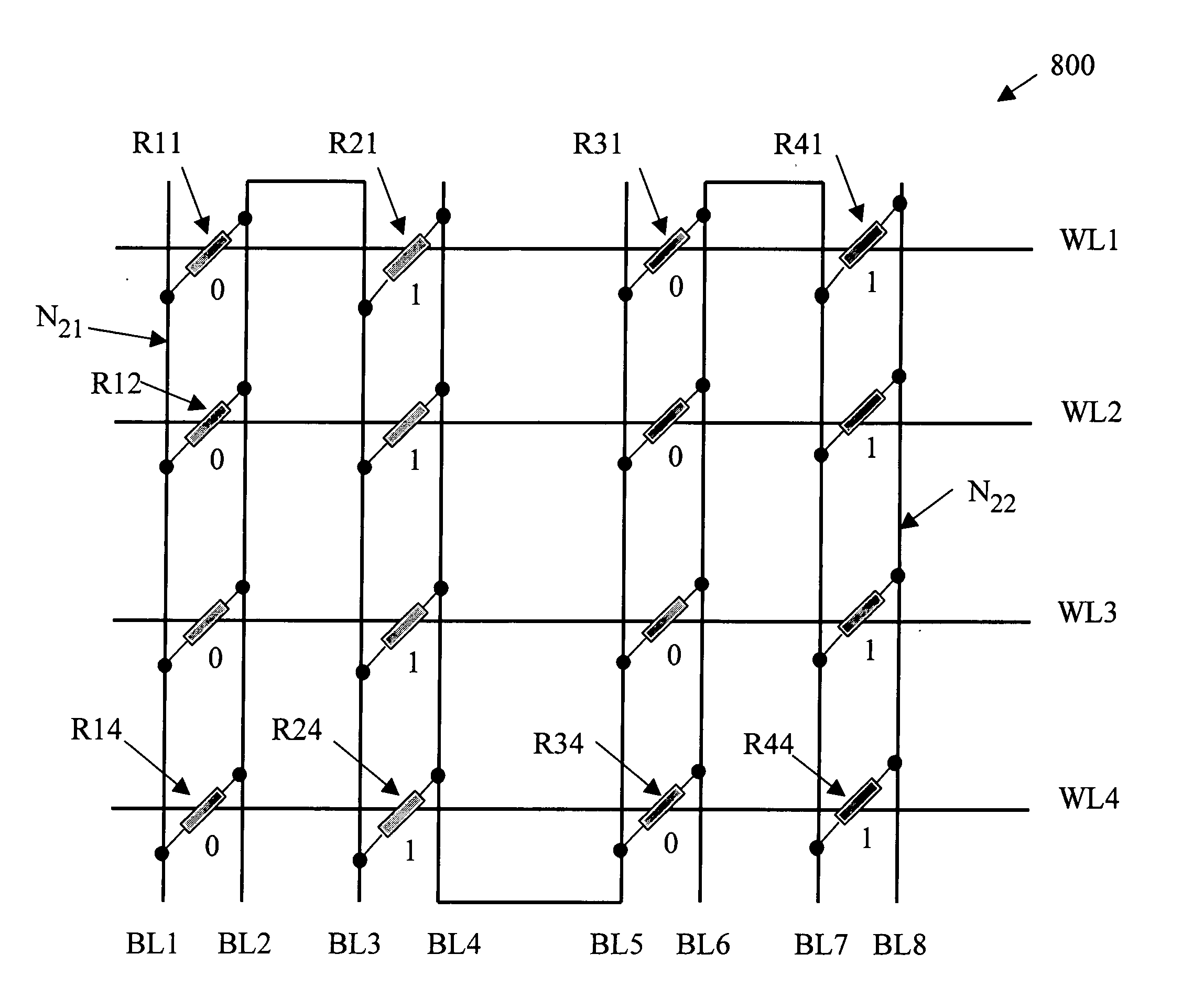
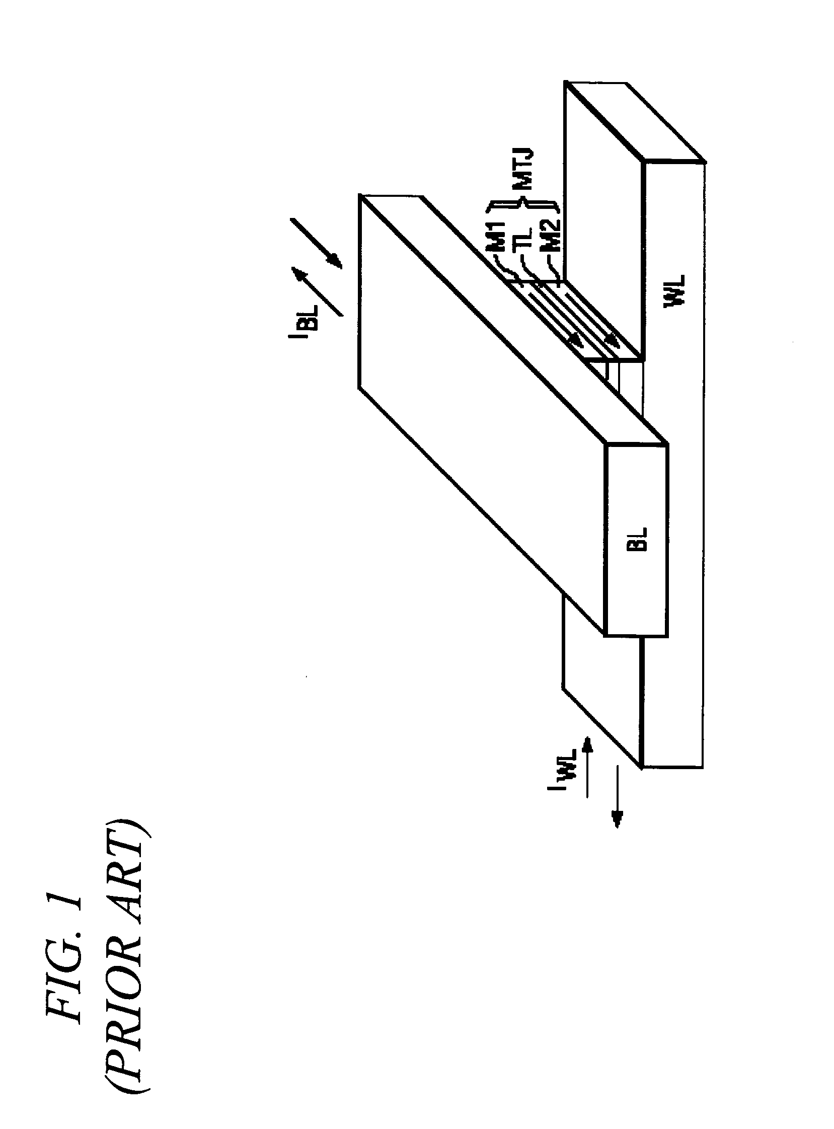
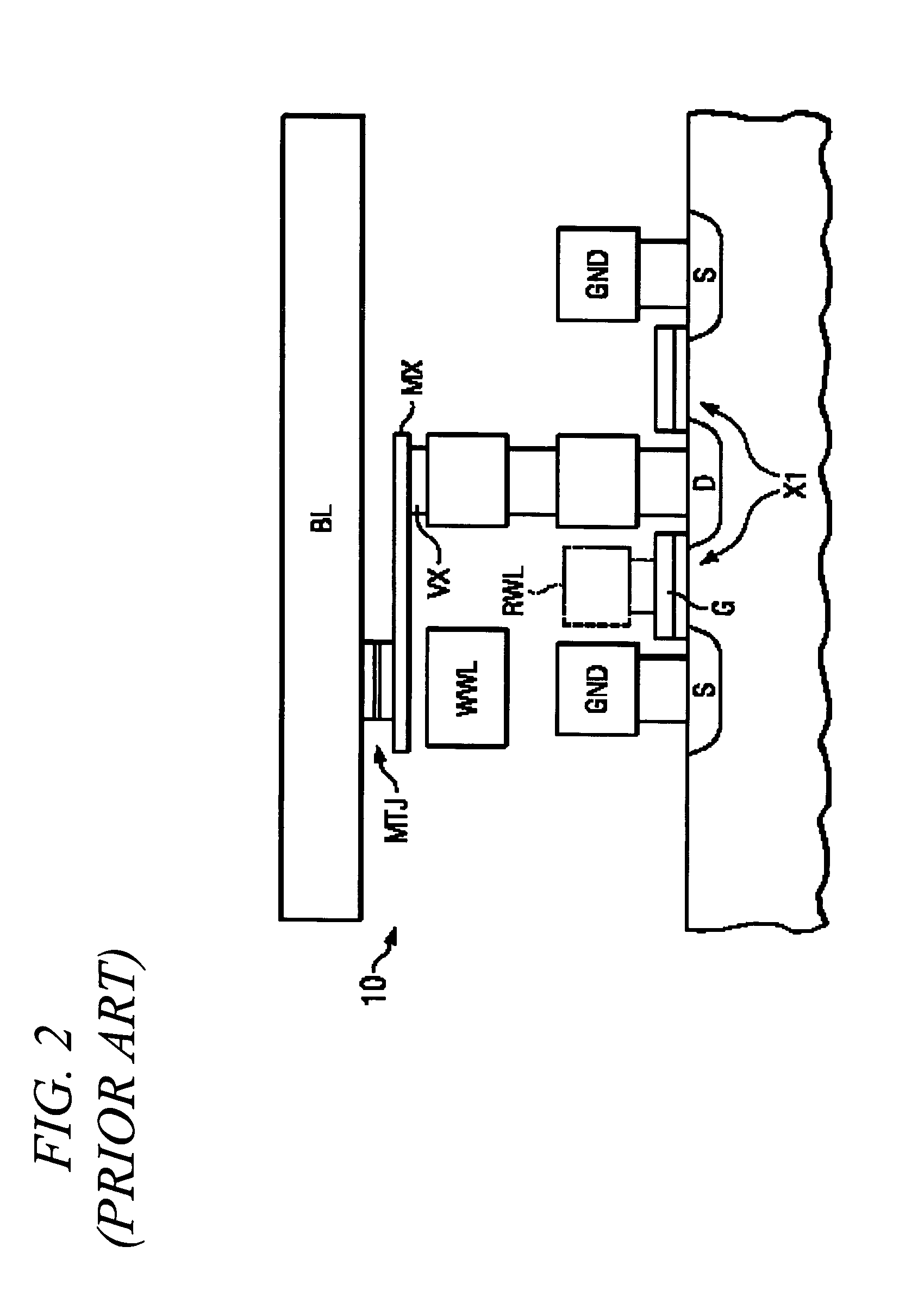
[0050] Embodiments of the present invention will be described with respect to preferred embodiments in a specific context, namely a FET MRAM device including a reference current source. The invention may also be applied, however, to resistive memory devices and other memory devices that include a current sense amplifier and a reference current source to detect the resistive state of memory cells. The current sense amplifier and the reference current source are also applicable in other applications where an unknown current is compared to a reference current in order to read ...


PUM


Abstract

A reference current source for a magnetic memory device is preferably configured with magnetic tunnel junction cells and includes more than four reference magnetic memory cells to improve reliability of the magnetic memory device and to reduce sensitivity at a device level to individual cell failures. The reference current source includes a large number of magnetic memory cells coupled in an array, and a current source provides a reference current dependent on the array resistance. In another embodiment a large number of magnetic memory cells are coupled to current sources that are summed and scaled to produce a reference current source. A current comparator senses the unknown state of a magnetic memory cell. In a further embodiment, an array of magnetic memory cells is configured to provide a non-volatile, adjustable resistance. In a further embodiment, the array of magnetic memory cells is configured with a tap to provide a non-volatile, adjustable potentiometer.

Description

CROSS-REFERENCE TO RELATED APPLICATIONS [0001] This application relates to co-pending and commonly assigned patent applications which are hereby incorporated herein by reference: Patent orAttorneySer. No.Filing DateIssue DateDocket No.10 / 326,367Dec. 20, 20022002 P 5007510 / 937,155Sep. 7, 20042004 P 5091110 / 925,487Aug. 25, 20042003 P 52584<xxx>2004 P 51925TECHNICAL FIELD [0002] Embodiments of the present invention relate generally to using multiple magnetic tunnel junction cells to improve the reliability of semiconductor memory devices, and more particularly, to reference current sources for sensing circuits for determining the resistive state of memory cells, and, further, to their use for configuring programmable, non-volatile resistors. BACKGROUND [0003] Semiconductors are used in integrated circuits for electronic applications, including radios, televisions, cell phones, and personal computing devices, as examples. One type of semiconductor device is a semiconductor storag...

Claims


Application Information

Patent Timeline
Patent Type & Authority Applications(United States)
IPC IPC(8): G11C11/00
CPCG11C7/067G11C7/14G11C11/16G11C29/028G11C29/50G11C29/50008G11C2207/063
Inventor BRAUN, DANIELKLOSTERMANN, ULRICH
Owner INFINEON TECH AG
Why Eureka
Try Eureka