Unlock instant, AI-driven research and patent intelligence for your innovation.

Power supply control circuit and controlling method thereof

a power supply control circuit and control circuit technology, applied in the direction of information storage, static storage, digital storage, etc., can solve the problems of large driving power required, difficult to apply the general voltage circuit to the semiconductor memory device, etc., and achieve the effect of accurate operation of the gio and high compression ra

Inactive Publication Date: 2006-05-04
SK HYNIX INC
View PDF15 Cites 4 Cited by
  • Summary
  • Abstract
  • Description
  • Claims
  • Application Information

AI Technical Summary

Benefits of technology

[0008] It is, therefore, an object of the present invention to provide a power supply control circuit and a control method thereof, capable of securing an accurate operation of a GIO in a burst data transmission having a high compression rate.
[0010] It is a further another object of the present invention to provide a power supply circuit and a controlling method thereof, in which a semiconductor memory device is not influenced due to a noise from other devices.
[0011] It is a still further another object of the present invention to provide a power supply circuit and a controlling method thereof, capable of effectively using a power.

Problems solved by technology

Therefore, a large amount of a driving power is required for driving the GIO bus.
Thus, it is difficult to apply the general voltage circuit to the semiconductor memory device.
Accordingly, in case where the above technology is applied to the DDR or DDR2 technology, that is, in case where a burst data transmission with a high compression rate is applied, a timing of loading data on the GIO bus is different from that of supplying a driving voltage to the GIO bus, resulting in an erroneous operation.

Method used


Image

  • Power supply control circuit and controlling method thereof
  • Power supply control circuit and controlling method thereof
  • Power supply control circuit and controlling method thereof

Examples


Embodiment Construction

[0031] Hereinafter, the present invention will be described in detail with reference to the accompanying drawings.

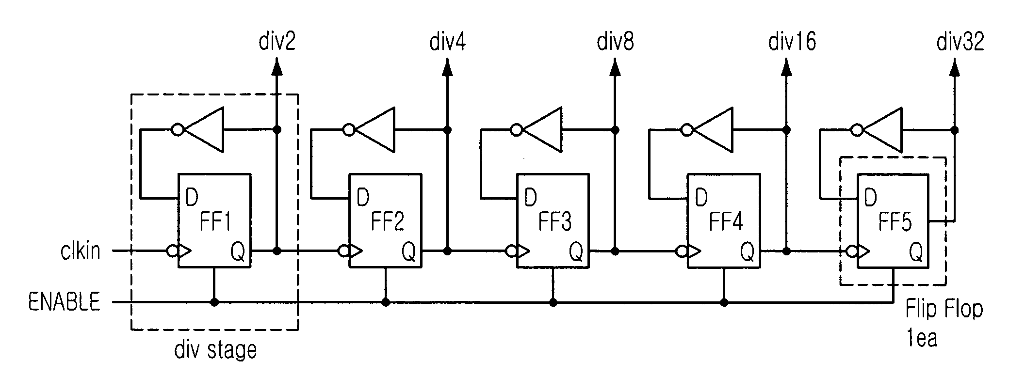
[0032]FIG. 5 is a power supply controlling circuit 100 of a semiconductor memory device incorporating therein a plurality of internal power suppliers in accordance with a preferred embodiment of the present invention.

[0033] Referring to FIG. 5, the inventive power supply controlling circuit 100 includes a power supply enable signal generator 110, a counter 120, a setting signal generator 130, a reset signal generator 140 and a counter controller 150. Herein, the counter 120 counts an input clock and outputting a counting completion signal after performing a counting operation in which the counter 120 is reset by receiving a read pulse RDP or a write pulse WTP. The power supply enable signal generator 110 outputs a power supply enable signal VGIOEN which is disabled by the counting completion signal of the counter 120. In the present invention, the power supply enable s...


PUM


Abstract

The present invention provides a power supply control circuit and a control method thereof, capable of securing an accurate operation of a GIO in a burst data transmission having a high compression rate. The power supply control circuit of a semiconductor memory device includes: a counter which is reset in response to a read command signal or a write command signal to count an input clock and then, to output a counting completion signal; and a power supply enable signal generator enabled in response to the read command signal or the write command signal and disabled in response to the counting completion signal, for generating a power supply enable signal.

Description

FIELD OF THE INVENTION [0001] The present invention relates to a power supply circuit for supplying a voltage to a data input / output circuit in a semiconductor memory device; and, more particularly, to a power supply circuit with a power supply controller for supplying a voltage to a global input / output (GIO) bus, and a controlling method thereof. DESCRIPTION OF RELATED ART [0002] A semiconductor memory device includes external input / output (I / O) pins for interfacing with an external circuit and a plurality of memory cells for storing data. In the semiconductor memory device, an area around the external I / O pins is called a peripheral area and an area around the memory cells is called a core area. [0003] In a structure of a semiconductor memory chip, the peripheral area and the core area are spaced apart from each other by a predetermined distance. The global I / O (GIO) bus consisting of I / O lines for data transmission between the peripheral area and the core area have considerable r...

Claims


Application Information

Patent Timeline
IPC IPC(8): G11C5/14G11C7/10
CPCG11C5/147G11C7/1048G11C7/1066G11C5/148G11C7/22
Inventor LEE, IHL-HO
Owner SK HYNIX INC