Design analysis workstation for analyzing integrated circuits

a workstation and integrated circuit technology, applied in the field of integrated circuit verification, can solve the problems of large amount of computation for analysis, large amount of time and manual labor required to reverse-engineer an ic, and high cost of owning and operating a scanning electron microscop

Inactive Publication Date: 2006-05-04
TECHINSIGHTS
View PDF6 Cites 19 Cited by
  • Summary
  • Abstract
  • Description
  • Claims
  • Application Information

AI Technical Summary

Problems solved by technology

In general, a vast amount of time and manual labor is required to reverse-engineer an IC.
In general, the scanning electron microscope is accurate but is expensive to own and operate.
These fringe effects can be interpreted by an experienced human analyst but require vast amounts of computation for analysis by a computer.
While the teachings of Suszko have merit, design and layout extraction are impeded by the handling and cross-correlation of the bulky transparencies.
Human enabled extraction of design and layout information from image-mosaics is lengthy.
However, Yu et al. fail to describe how multiple image-mosaics, each representing a different step in the deconstruction of an IC, are manipulated in order to extract design and layout information concurrently therefrom.
While such automated systems are ingenious, it is debatable whether such automated design and layout extraction methods are superior to or more economical than human driven processes.

Method used


Image

  • Design analysis workstation for analyzing integrated circuits
  • Design analysis workstation for analyzing integrated circuits
  • Design analysis workstation for analyzing integrated circuits

Examples


Embodiment Construction

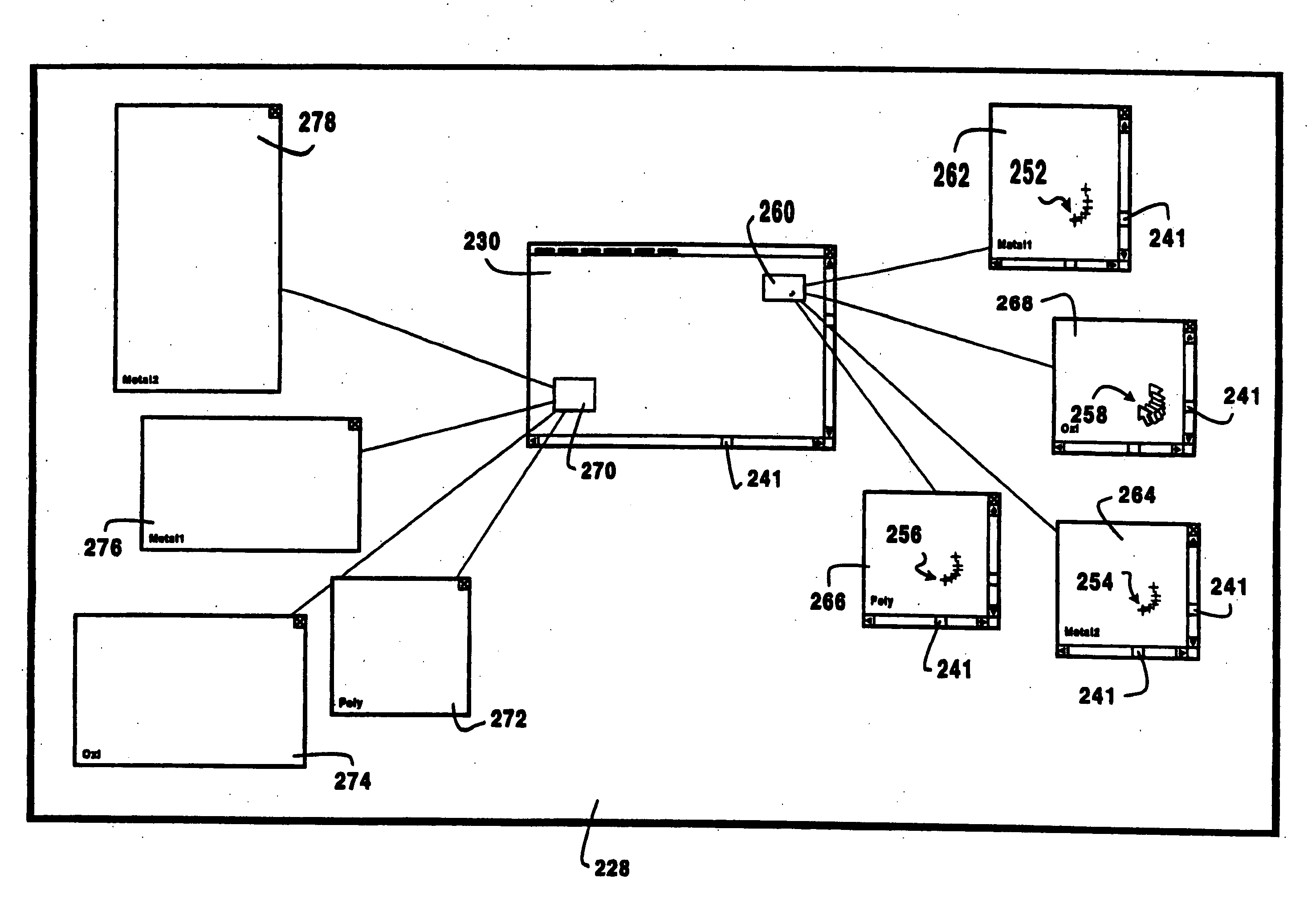
[0036] The invention provides a design analysis workstation to facilitate the extraction of component and component interconnection information from image-mosaics captured during the deconstruction of an integrated circuit. The design analysis workstation displays a plurality of image-mosaics concurrently in respective independent mosaic-views. The mosaic-views are synchronized to display the same area of the respective image-mosaics. Design information is extracted by recreating all or parts of the components and component interconnections as schematics drawn on one or more annotation overlays displayed over one or more of the mosaic-views.

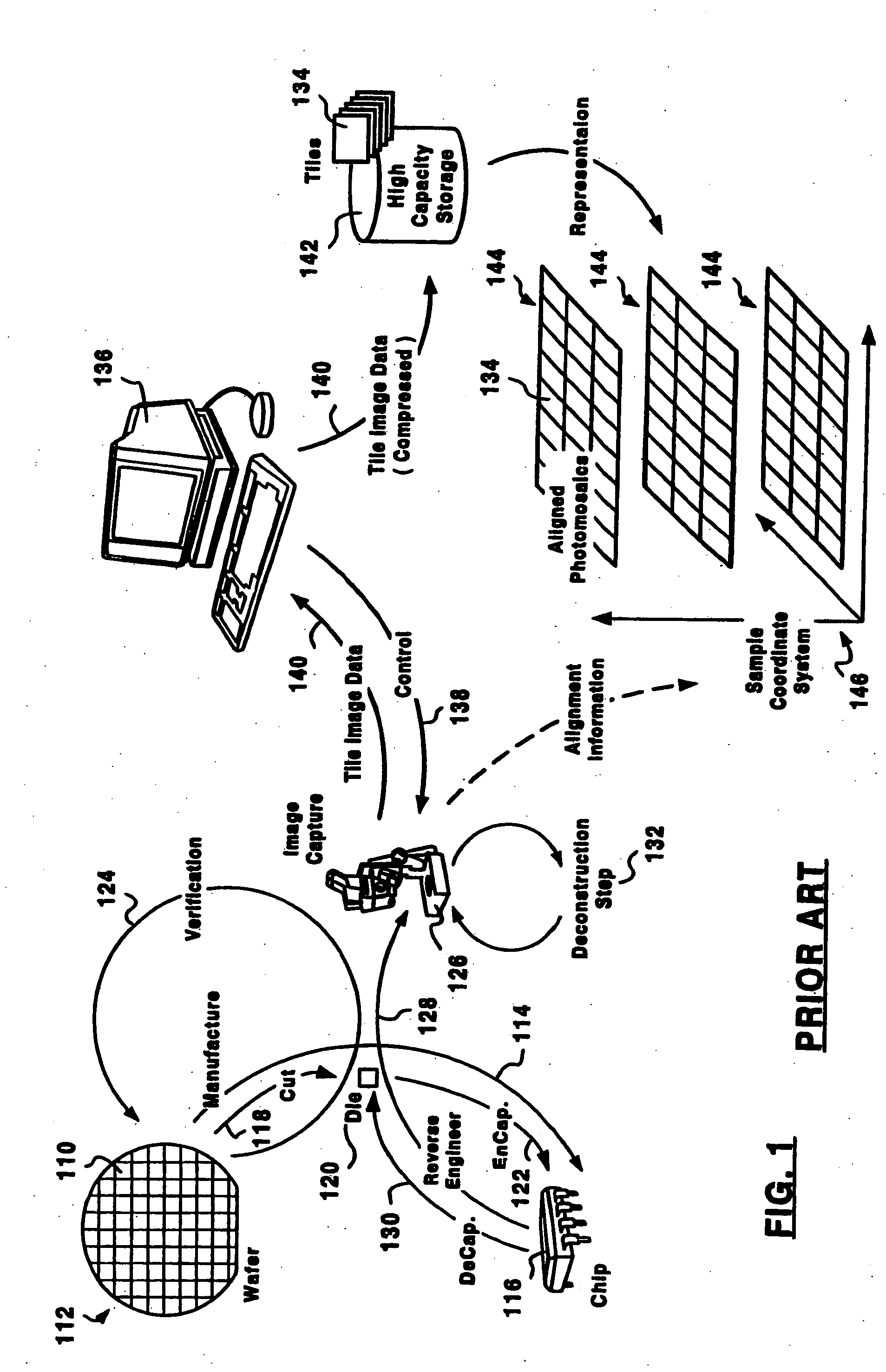
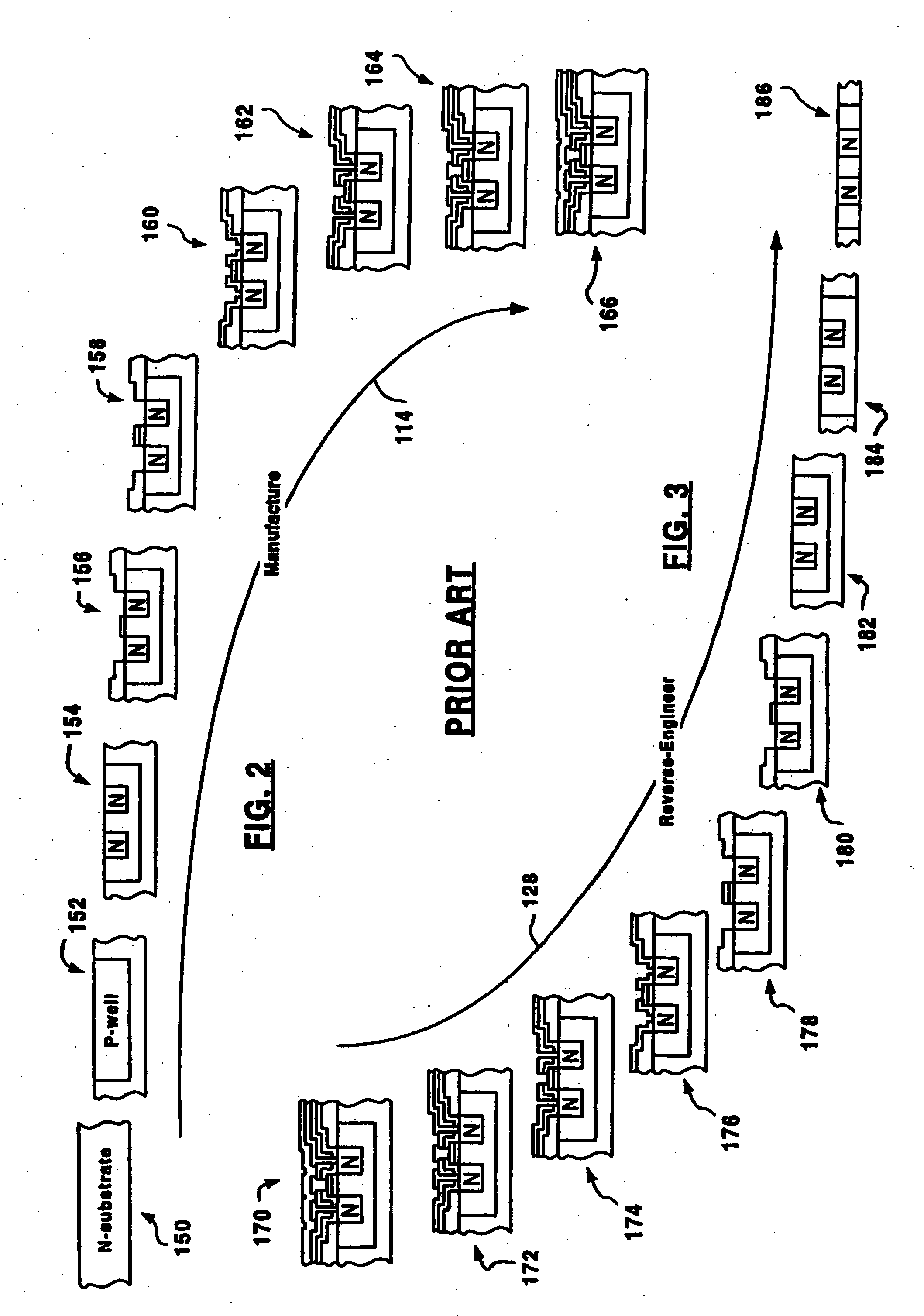
[0037]FIG. 1 is a work-flow diagram showing an overview of an exemplary prior art process by which image-mosaics representative of steps in the deconstruction of a semi-conductor integrated circuit (IC) are acquired. IC's 110 are fabricated on a wafer 112. The wafer 112 comprises a mono-crystalline silicon substrate which is a natural insulator....


PUM


Abstract

A design analysis workstation for performing design analysis of integrated circuits provides facilities for extracting design and layout information from digital image-mosaics captured during deconstruction of an integrated circuit. The design analysis workstation enables propagation of signal information from an annotation object having a signal property to at least one connected annotation object in order to point to errors in the design analysis.

Description

CROSS-REFERENCE TO RELATED APPLICATIONS [0001] This application is a division of U.S. patent application Ser. No. 10 / 717,460 which is a divisional of Ser. No. 09 / 927,551, which is a continuation of U.S. patent application Ser. No. 09 / 690,813, filed Oct. 18, 2000, and now abandoned.MICROFICHE APPENDIX [0002] Not Applicable. TECHNICAL FIELD [0003] The invention relates to the field of integrated circuit verification, and in particular to methods and apparatus for extracting design and layout information from integrated circuits. BACKGROUND OF THE INVENTION [0004] In the semiconductor industry it is often necessary to physically analyze semiconductor integrated circuits (ICs) for the purposes of product reliability assurance, design validation and identification of device structural patterns. ICs are analyzed to extract design and / or layout information therefrom. This process is known as reverse-engineering. Reverse-engineering is also part of the test and development process in the ma...

Claims


Application Information

Patent Timeline
Patent Type & Authority Applications(United States)
IPC IPC(8): G06F17/50G06F9/455G06T7/00
CPCG06F17/5081G06T7/0006G06T7/001G06T7/0022G06T2200/24G06T2200/32G06T2207/30148G06T7/97G06F30/398
Inventor SKOLL, DAVID F.LUDLOW, TERRYELVIDGE, JULIA
Owner TECHINSIGHTS
Why Eureka
Try Eureka