
Substrate processing apparatus and substrate processing method

a substrate processing and substrate technology, applied in the direction of photomechanical equipment, instruments, photosensitive materials, etc., can solve the problems of defective dimension, defective shape of exposure pattern, and inability to make resist pattern finer than

Inactive Publication Date: 2006-05-11
THE UNITED STATES OF AMERICA AS REPRESENTED BY THE SECRETARY OF THE NAVY +1
View PDF6 Cites 39 Cited by
  • Summary
  • Abstract
  • Description
  • Claims
  • Application Information

AI Technical Summary

Benefits of technology

[0011] It is an object of the invention to provide a substrate processing apparatus and a substrate processing method capable of preventing a component of a processing liquid on a substrate from being eluted in a liquid in an exposure device.

Problems solved by technology

With such conventional exposure devices, however, the line width of an exposure pattern is determined by the wavelength of the light source of an exposure device, thus making it impossible to make a resist pattern finer than that.
The resist component eluted in the liquid remains on a surface of the substrate, which may become the cause of a defect.
This may cause a defective dimension and a defective shape of the exposure pattern.

Method used


Image

  • Substrate processing apparatus and substrate processing method
  • Substrate processing apparatus and substrate processing method
  • Substrate processing apparatus and substrate processing method

Examples


Embodiment Construction

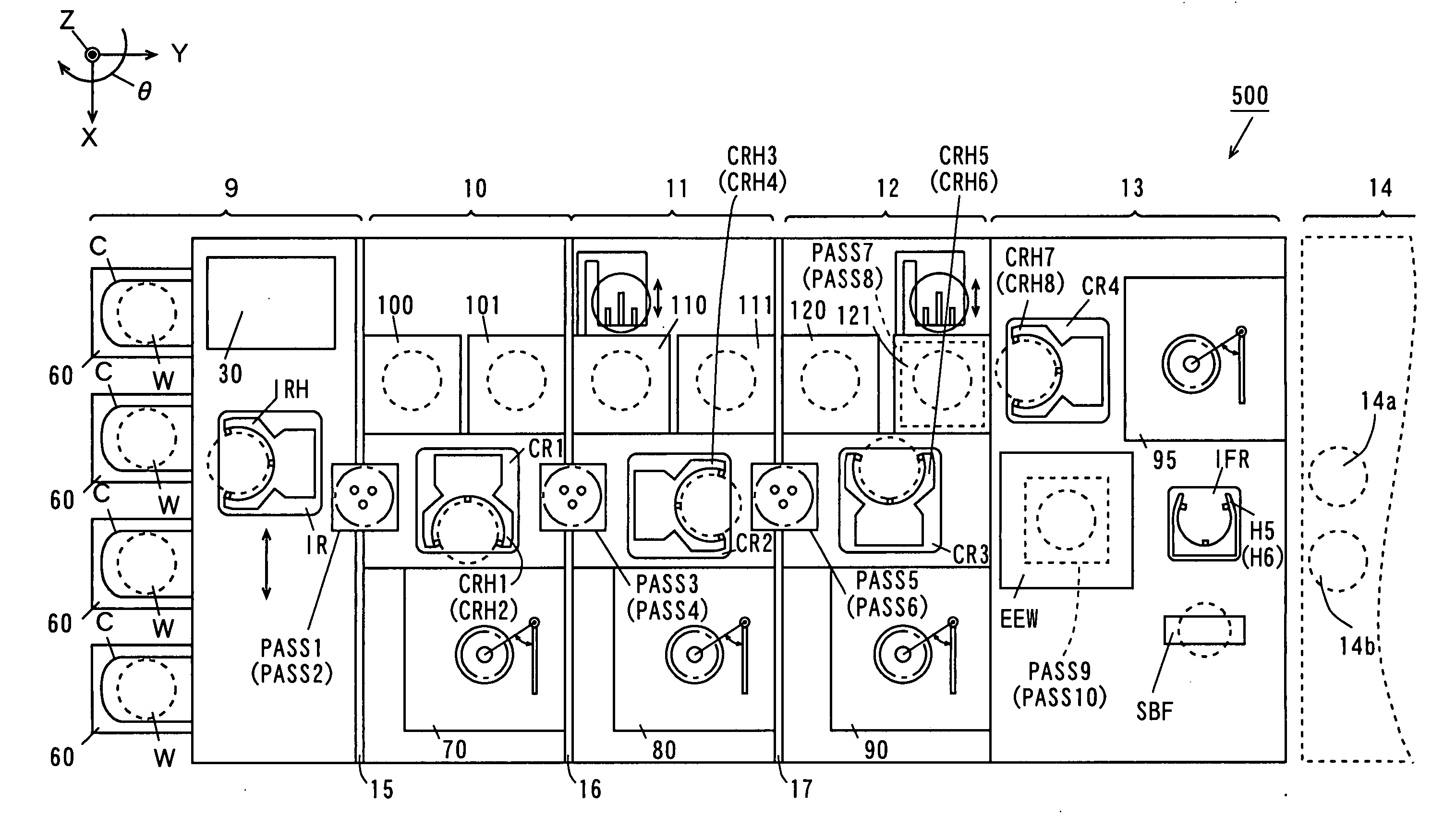
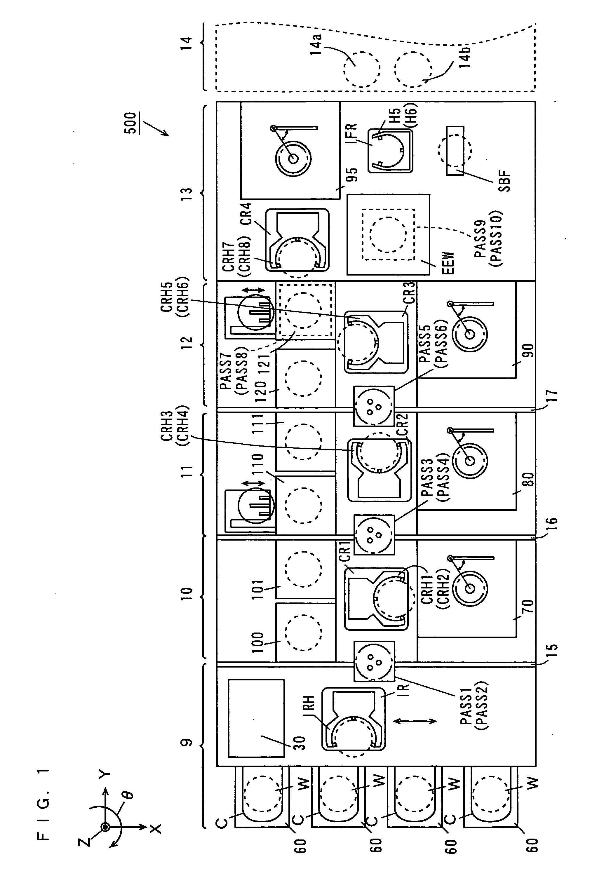
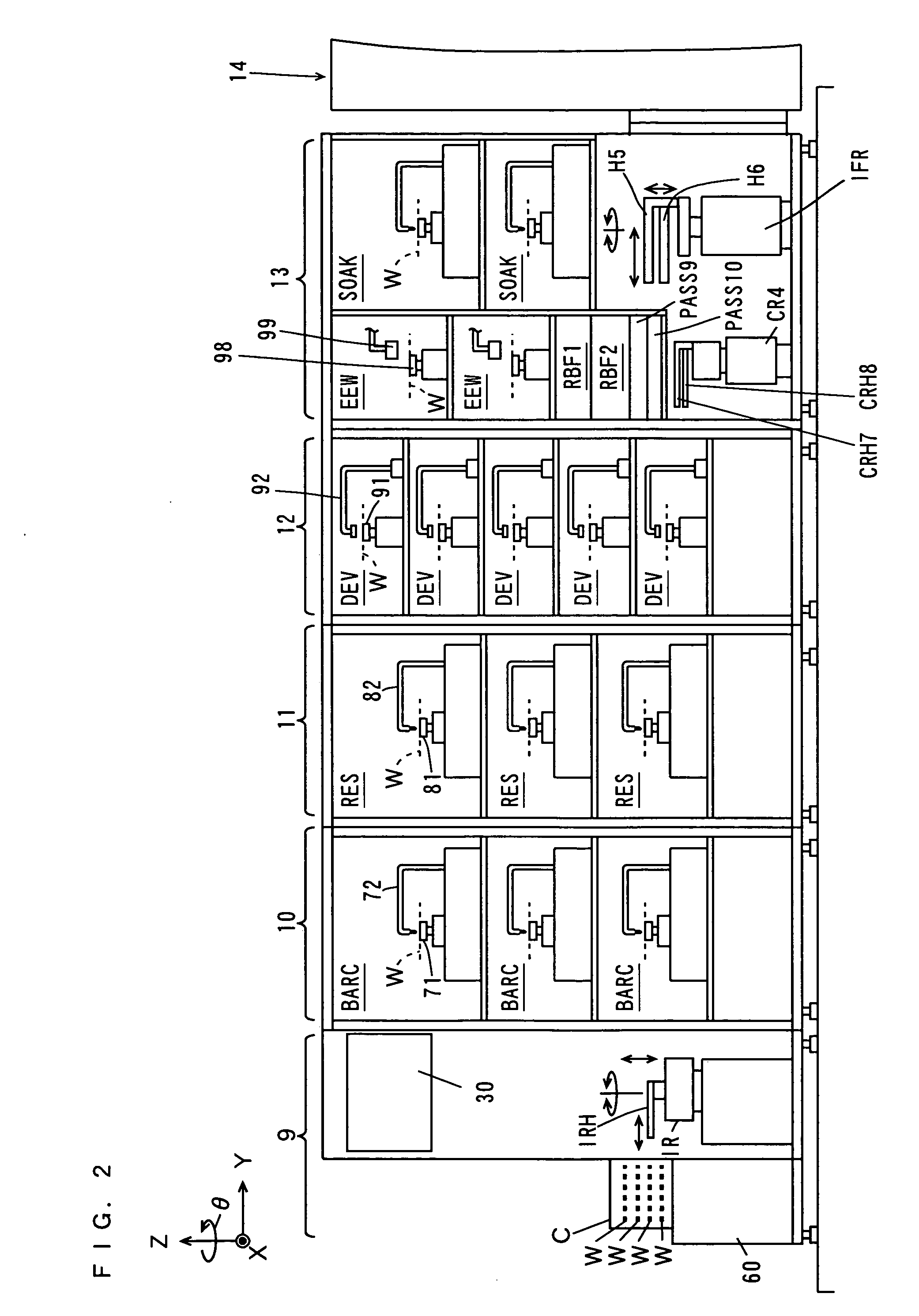
[0101] A substrate processing apparatus according to an embodiment of the invention will be described with reference to the drawings. A substrate as used in the specification includes a semiconductor substrate, a substrate for a liquid crystal display, a substrate for a plasma display, a glass substrate for a photomask, a substrate for an optical disk, a substrate for a magnetic disk, a substrate for a magneto-optical disk, and a substrate for a photomask.

[0102]FIG. 1 is a plan view of the semiconductor laser apparatus according to the embodiment of the invention.

[0103] Each of FIG. 1 and the subsequent drawings is accompanied by the arrows that indicate X, Y, and Z directions perpendicular to one another for clarification of positions. The X and Y directions are perpendicular to each other in a horizontal plane, and the Z direction corresponds to the vertical direction. In each of the directions, the direction toward an arrow is defined as + direction, and the opposite direction ...


PUM


Abstract

A substrate processing apparatus comprises an indexer block, an anti-reflection film processing block, a resist film processing block, a development processing block, and an interface block. An exposure device is arranged adjacent to the interface block. The interface block comprises washing processing units and an interface transport mechanism. Before a substrate is subjected to exposure processing by the exposure device, the substrate is transported to a washing processing unit by the interface transport mechanism. The substrate is washed and dried by the washing processing unit.

Description

BACKGROUND OF THE INVENTION [0001] 1. Field of the Invention [0002] The present invention relates to a substrate processing apparatus and a substrate processing method for applying processing to substrates. [0003] 2. Description of the Background Art [0004] A substrate processing apparatus is used to apply a variety of processings to substrates such as semiconductor substrates, substrates for use in liquid crystal displays, plasma displays, optical disks, magnetic disks, magneto-optical disks, photomasks, and other substrates. [0005] Such a substrate processing apparatus typically applies a plurality of successive processings to a single substrate. The substrate processing apparatus as described in JP 2003-324139 A comprises an indexer block, an anti-reflection film processing block, a resist film processing block, a development processing block, and an interface block. An exposure device is arranged adjacent to the interface block as an external device separate from the substrate p...

Claims


Application Information

Patent Timeline
IPC IPC(8): G03D5/00
CPCG03F7/7075G03F7/70991Y10S438/906Y10S438/908
Inventor YASUDA, SCHUICHIKANAOKA, MASASHIKANEYAMA, KOJIMIYAGI, TADASHISHIGEMORI, KAZUHITOASANO, TORUHISAI, AKIHIROKOBAYASHIOKUMURA, TSUYOSHI
Owner THE UNITED STATES OF AMERICA AS REPRESENTED BY THE SECRETARY OF THE NAVY
Features
  • Generate Ideas
  • Intellectual Property
  • Life Sciences
  • Materials
  • Tech Scout
  • Unparalleled Data Quality
  • Higher Quality Content
  • 60% Fewer Hallucinations
Learn More