Process for fabricating chip embedded package structure

a technology of embedded package and manufacturing process, which is applied in the direction of individual semiconductor device testing, semiconductor/solid-state device testing/measurement, instruments, etc., can solve the problems of reducing the reliability of the subsequently formed multi-layered interconnection structure, complex process but trivial, etc., to improve structural coplanarity and package reliability, shorten processing time, and increase positional accuracy

Active Publication Date: 2006-05-18
VIA TECH INC
View PDF5 Cites 39 Cited by
  • Summary
  • Abstract
  • Description
  • Claims
  • Application Information

AI Technical Summary

Benefits of technology

[0013] Accordingly, the present invention is directed to a chip embedded package structure capable of shortening the processing time, increasing positional accuracy, improving structural coplanarity and package reliability, and yield of the packaging.
[0015] In brief, alignment marks are pre-fabricated on the tape in the present embodiment of the present invention so that the alignment marks can be used to attach the chip, form the conductive vias and fabricate the multi-layered interconnection structure. Furthermore, there is no need to remove the tape throughout the packaging process. Consequently, the processing time of the package is reduced, the positioning accuracy and yield are increased and the structural coplanarity and reliability of the package are improved.

Problems solved by technology

The tape needs to be torn away and the surface needs to be cleaned so that the process is complicated but trivial.
Moreover, after tearing the tape away from the chip and the stiffener, coplanarity between the chip and the stiffener is hard to maintain.
Ultimately, this may reduce the reliability of the subsequently formed multi-layered interconnection structure.
In addition, no alignment marks are set up for performing laser drilling or photolithographic process during the fabrication of the multi-layered interconnection structure.
Without any alignment mark to enhance processing accuracy, it is difficult to increase the overall yield of the packaging.

Method used


Image

  • Process for fabricating chip embedded package structure
  • Process for fabricating chip embedded package structure
  • Process for fabricating chip embedded package structure

Examples


Embodiment Construction

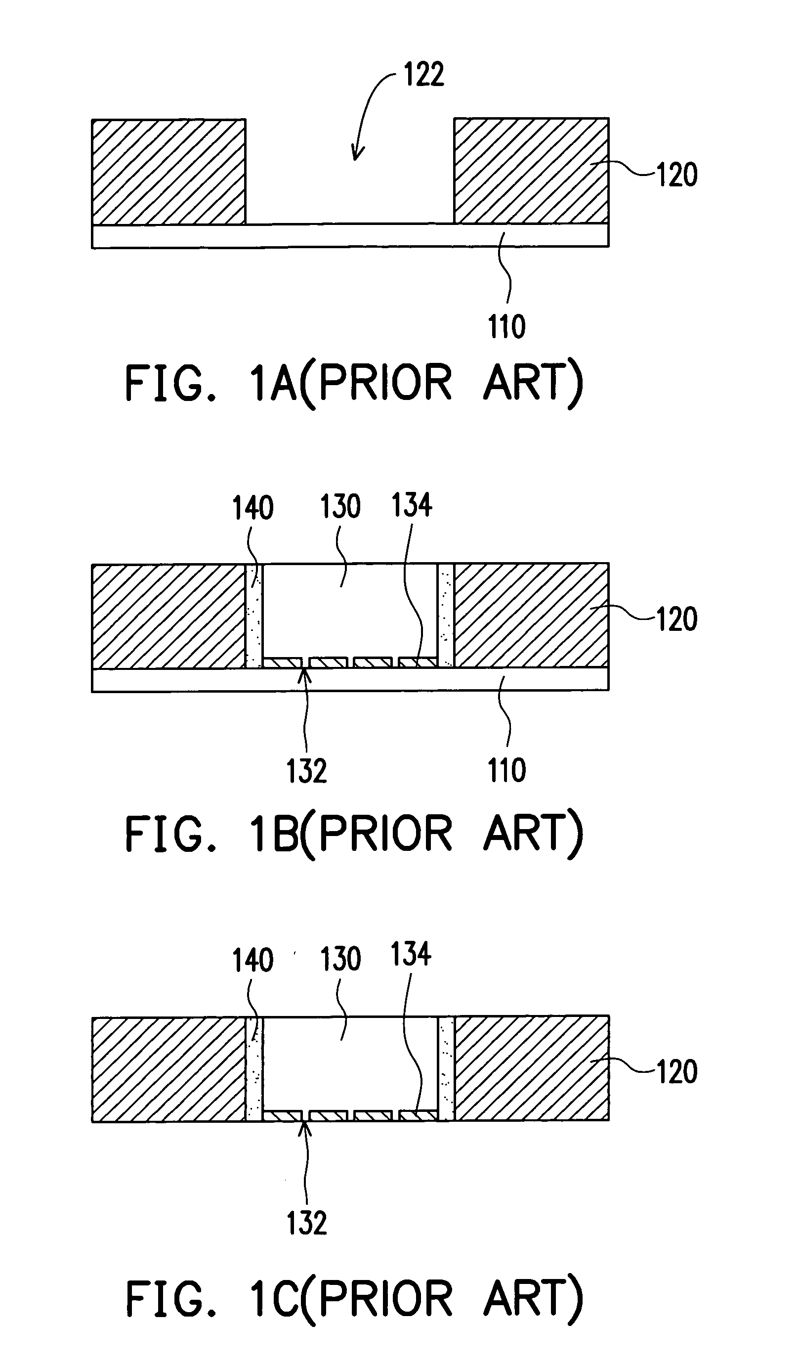
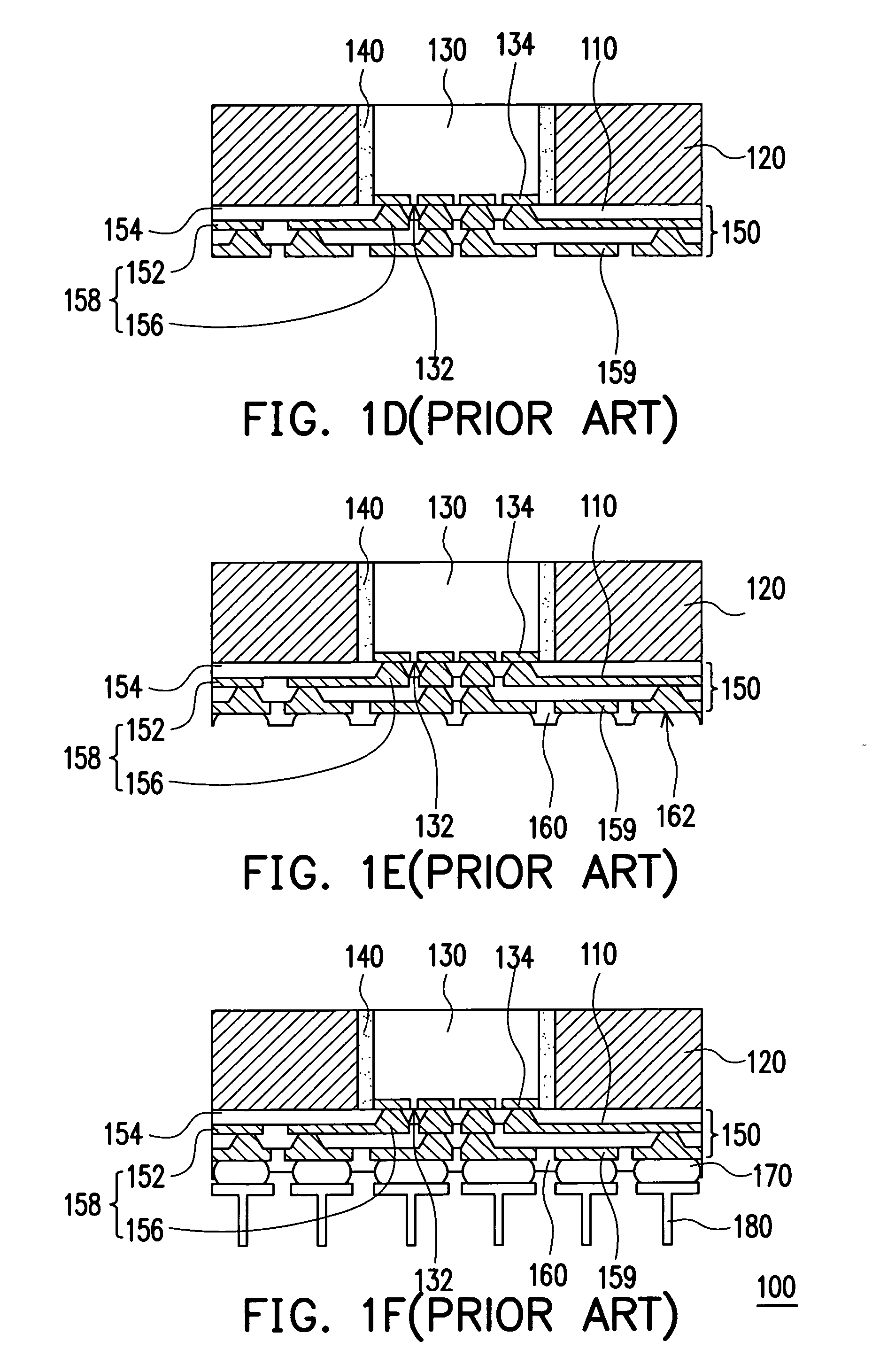
[0021] Reference will now be made in detail to the present preferred embodiments of the invention, examples of which are illustrated in the accompanying drawings. Wherever possible, the same reference numbers are used in the drawings and the description to refer to the same or like parts.

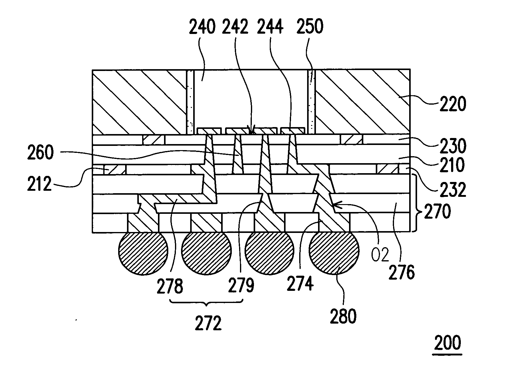
[0022]FIGS. 2A through 2G are schematic cross-sectional views showing the steps of fabricating a chip embedded package structure according to one embodiment of the present invention. First, as shown in FIG. 2A, a tape 210 is provided. The tape 210 is a polyimide (PI) tape, for example. The tape 210 comprises at least an alignment mark 212 (four alignment marks in the illustration) on the surface of the tape 210. These alignment marks 212 are not limited to any one side of the tape 210. In general, the alignment marks 212 can be disposed on both sides of the tape 210.

[0023] The tape 210 may further comprise a circuit layer 216 disposed on a surface that will not come in contact with a subsequently ...


PUM


Abstract

A process for fabricating a chip embedded package structure is provided. A stiffener is disposed on a tape. A chip is disposed on the tape inside a chip opening of the stiffener such that an active surface of the chip faces the tape. Through holes are formed passing the tape and exposing bonding pads of the chip on the active surface respectively. Conductive material is deposited into the though holes to form a plurality of conductive vias which are connected to the bonding pads respectively. A multi-layered interconnection structure is formed on the tape on the opposite of the chip, wherein the multi-layered interconnection structure comprises an inner circuit which is connected to the conductive vias, and the inner circuit has a plurality of metallic pads on a surface of the multi-layered interconnection structure away from the tape.

Description

CROSS-REFERENCE TO RELATED APPLICATION [0001] This application is a continuation of a prior application serial no. U.S. Ser. No. 10 / 994,043, filed on Nov. 18, 2004, now pending, which claims the priority benefit of Taiwan application Serial No. 93113134, filed on May 11, 2004. All disclosures are incorporated herewith by reference.BACKGROUND OF THE INVENTION [0002] 1. Field of the Invention [0003] The present invention relates to a process for fabricating a chip package structure. More particularly, the present invention relates to a process for fabricating a chip embedded package structure. [0004] 2. Description of Related Art [0005] In this electronic age, multi-functional, highly integrated, miniaturized, inexpensive devices with a high processing speed are in great demand. To meet this trend, chip packages are also highly miniaturized and densified. In the conventional ball grid array (BGA) packaging technique, a package substrate is often used as a carrier for an integrated cir...

Claims


Application Information

Patent Timeline
Patent Type & Authority Applications(United States)
IPC IPC(8): H01L21/48H01L23/31H01L23/48H01L23/538H01L23/544
CPCH01L21/6835H01L2224/16235H01L23/544H01L2223/54473H01L2224/04105H01L2224/20H01L2924/14H01L2924/15174H01L2924/15311H01L2924/15312H01L2924/18162H01L2924/01033H01L24/19H01L2224/0401H01L23/5389H01L2924/12042H01L2224/12105H01L2224/92144H01L2224/83132H01L2224/32225H01L2924/00
Inventor CHANG, WEN-YUAN
Owner VIA TECH INC
Why Eureka
Try Eureka