Automatic fault-testing of logic blocks using internal at-speed logic-BIST

a logic block and fault-testing technology, applied in the field of automatic fault-testing of logic blocks, can solve the problems of failure to detect connectivity failures, tests performed at speeds that are slower than the intended operational speed of digital logic blocks, and tests performed at slower speeds

Active Publication Date: 2006-05-18
TAMIRAS PER PTE LTD LLC
View PDF6 Cites 11 Cited by
  • Summary
  • Abstract
  • Description
  • Claims
  • Application Information

AI Technical Summary

Benefits of technology

[0004] To achieve the foregoing and other objects and according to the purpose of the present invention, what is provided is a system and method for automatic fault-testing of a logic block and the interfaces of a semiconductor device (chip), using an at-speed logic-BIST circuit internal to the chip. Following an initialization of internal storage elements such as flip-flops or static random-access memories (SRAMs), a set of test signals are generated for processing by the logic block. The output of the logic block is accumulated into a test signature and compared to a reference signature to detect faults. Testing can be performed on an ATE using a simple test vector, and can be performed by a field engineer on the actual board comprising the chip. The ATE vector is simple, since it only needs to trigger the logic-BIST circuit without bothering about external timing constraints.

Problems solved by technology

Although this approach works, the tests are performed at speeds that are slower than the intended operational speed of the digital logic block under test.
In addition, such tests generally do not test the macros interface to the digital logic.
Hence, since the interfaces between macros and logic are generally tested individually, failures of the connectivity may not be detected.
Furthermore, a complex ATE interface does not allow for convenient testing of a chip in the field by a field engineer.

Method used


Image

  • Automatic fault-testing of logic blocks using internal at-speed logic-BIST
  • Automatic fault-testing of logic blocks using internal at-speed logic-BIST
  • Automatic fault-testing of logic blocks using internal at-speed logic-BIST

Examples


Embodiment Construction

[0011] In the following description, numerous specific details are set forth in order to provide a thorough understanding of the present invention. It will be understood, however, to one skilled in the art, that the present invention may be practiced without some or all of these specific details. In other instances, well known hardware design, operation and testing processes have not been described in detail in order not to unnecessarily obscure the present invention.

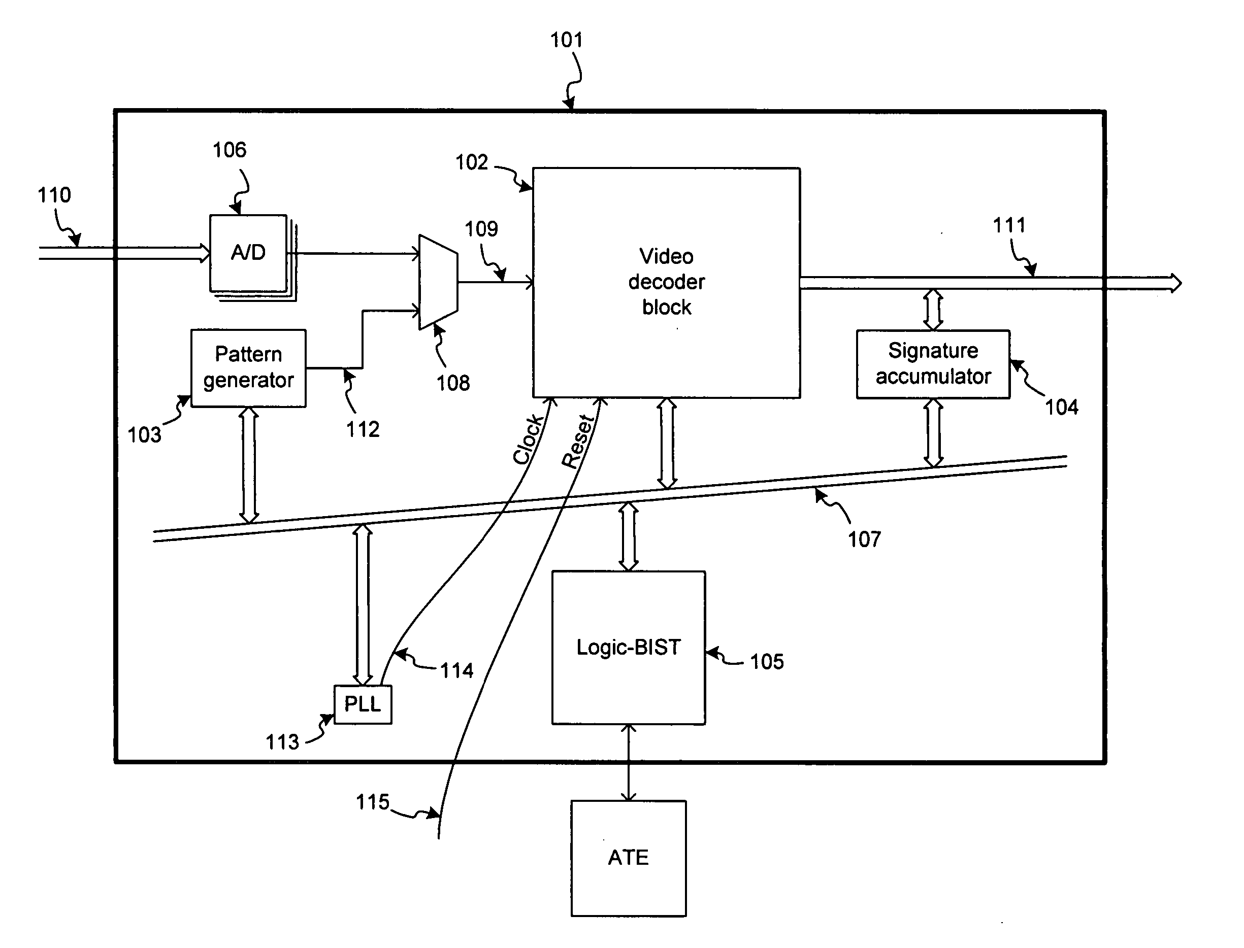
[0012] Accordingly, what is provided is a system and method for automatic fault-testing of the logic and the interfaces of a semiconductor device (chip), using an at-speed logic-BIST (Built-In Self Test) circuit internal to the chip. The invention allows testing to be performed on an ATE using a simple test vector. It also allows a field engineer to perform system-level tests on the actual board comprising the chip whenever a doubt as to the functionality of the chip arises. The ATE vector is simple, since it only need...


PUM


Abstract

System and method for automatic fault-testing of a logic block and the interfaces of macros with logic gates inside a chip, using an at-speed logic-BIST internal to the chip. Following an initialization of internal storage elements, a set of test signals are generated and processed by the logic block. The output of the logic block is accumulated into a signature and compared to a reference signature to detect faults. Testing can be performed on an ATE (Automatic Test Equipment) using a simple test vector, or can be performed by a field engineer on the actual board comprising the chip.

Description

BACKGROUND OF THE INVENTION [0001] The present invention relates generally to hardware testing and, more particularly, to automatic at-speed fault-testing of logic blocks using logic-BIST (Built-In Self Test) circuits. [0002] Testing of digital logic blocks is commonly performed using automatic testing equipment (ATE) and scan-chains in the digital logic block. Although this approach works, the tests are performed at speeds that are slower than the intended operational speed of the digital logic block under test. Thus, logic which fails at-speed or at desired speeds but passes at low speeds is not detected. In addition, such tests generally do not test the macros interface to the digital logic. Hence, since the interfaces between macros and logic are generally tested individually, failures of the connectivity may not be detected. Furthermore, a complex ATE interface does not allow for convenient testing of a chip in the field by a field engineer. [0003] Accordingly, a system and met...

Claims


Application Information

Patent Timeline
Patent Type & Authority Applications(United States)
IPC IPC(8): G01R31/28
CPCG01R31/318552G01R31/3187G01R31/3177G01R31/3183
Inventor MUSHIRABAD, VENKAT CHARYSHETTIGARA, RAJANATHA
Owner TAMIRAS PER PTE LTD LLC
Why Eureka
Try Eureka