Vertical probe card and method for using the same

a technology of vertical probe and probe card, which is applied in the direction of solid-state devices, instruments, and semiconductor/solid-state device details. it can solve the problems of wasting time and money when bad dies are packaged, manufacturing wafers consume the most time in the process of manufacturing ic products, and the cost of testing is an important component of the total cost of producing ics

Inactive Publication Date: 2005-03-01
SCS HIGHTECH
View PDF6 Cites 37 Cited by
  • Summary
  • Abstract
  • Description
  • Claims
  • Application Information

AI Technical Summary

Benefits of technology

Another object of the present invention is to provide an apparatus and a method for testing dies on an integrated circuit wafer with more accurate results.
A further object of the present invention is to provide an apparatus and a method that can test integrated circuit devices with very high frequency signals and still achieve accurate results.

Problems solved by technology

Besides, the cost of testing is an important component of the total cost of producing ICs.
Such a process does not sort out bad dies before packaging and thus wastes time and money when bad dies are packaged.
Manufacturing wafers consumes the most time in the process of manufacturing IC products.
It is consequently normal to produce a number of surplus wafers at the first stage of IC production in anticipation of failures because it is generally not acceptable to start replacement wafer production when the IC failure rate is known.
The result is that a manufacturer will keep a larger stock of wafers on hand, which increases costs.
In a multi-chip module any bad chip will result in the discard of the entire module.
The testing thus experiences the greater complexity of the module and achieves less reliable results.
The effect is higher testing costs, longer research and development cycles and costs, and a higher risk of returned goods.
If individual dies were sorted before they were packaged, testing of the packaged multi-chip module would only need to identify damage caused by the packaging process, limiting the above-mentioned drawbacks.
Secondly, due to its structural strength requirement, the cantilever type probes 12 must be made relatively thick so that the density of the probes 12 is limited.
Consequently the number of I / O terminals of the die to be tested is also limited or the die must be over-sized.
Thirdly, cantilever type probe cards are disadvantageous for high frequency testing.
This results in serious electromagnetic interference (“EMI”) when high frequency test signals are applied.
Moreover, the different length of these wires also causes impedance mismatches that are detrimental to high frequency access time testing.
The major problem of such a device is that the dimensional stability of the membrane is not sufficient to allow contacts to be made to pads on a full wafer during a burn-in temperature cycle.

Method used


Image

  • Vertical probe card and method for using the same
  • Vertical probe card and method for using the same
  • Vertical probe card and method for using the same

Examples


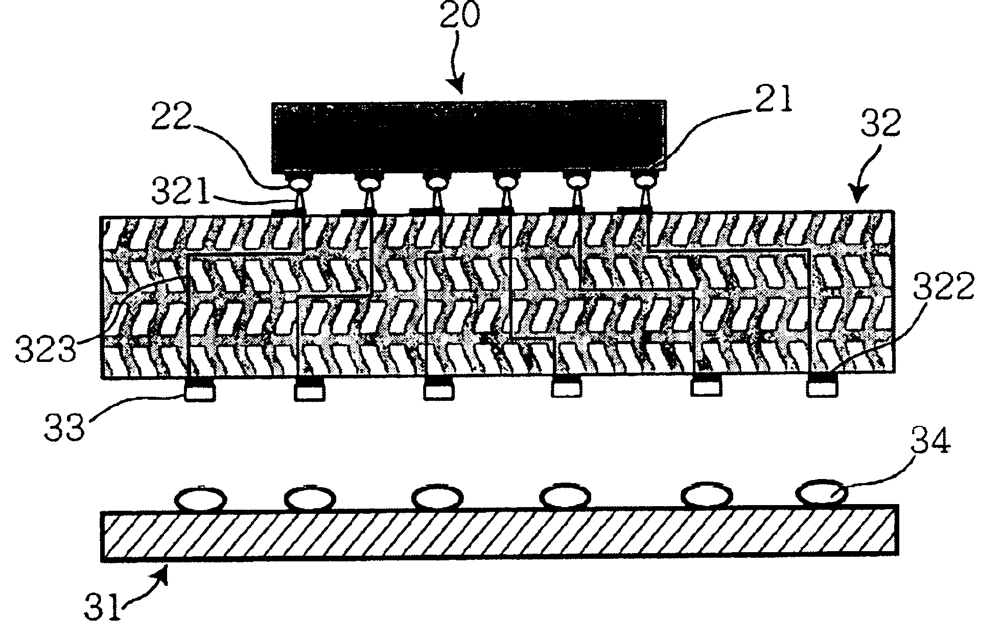
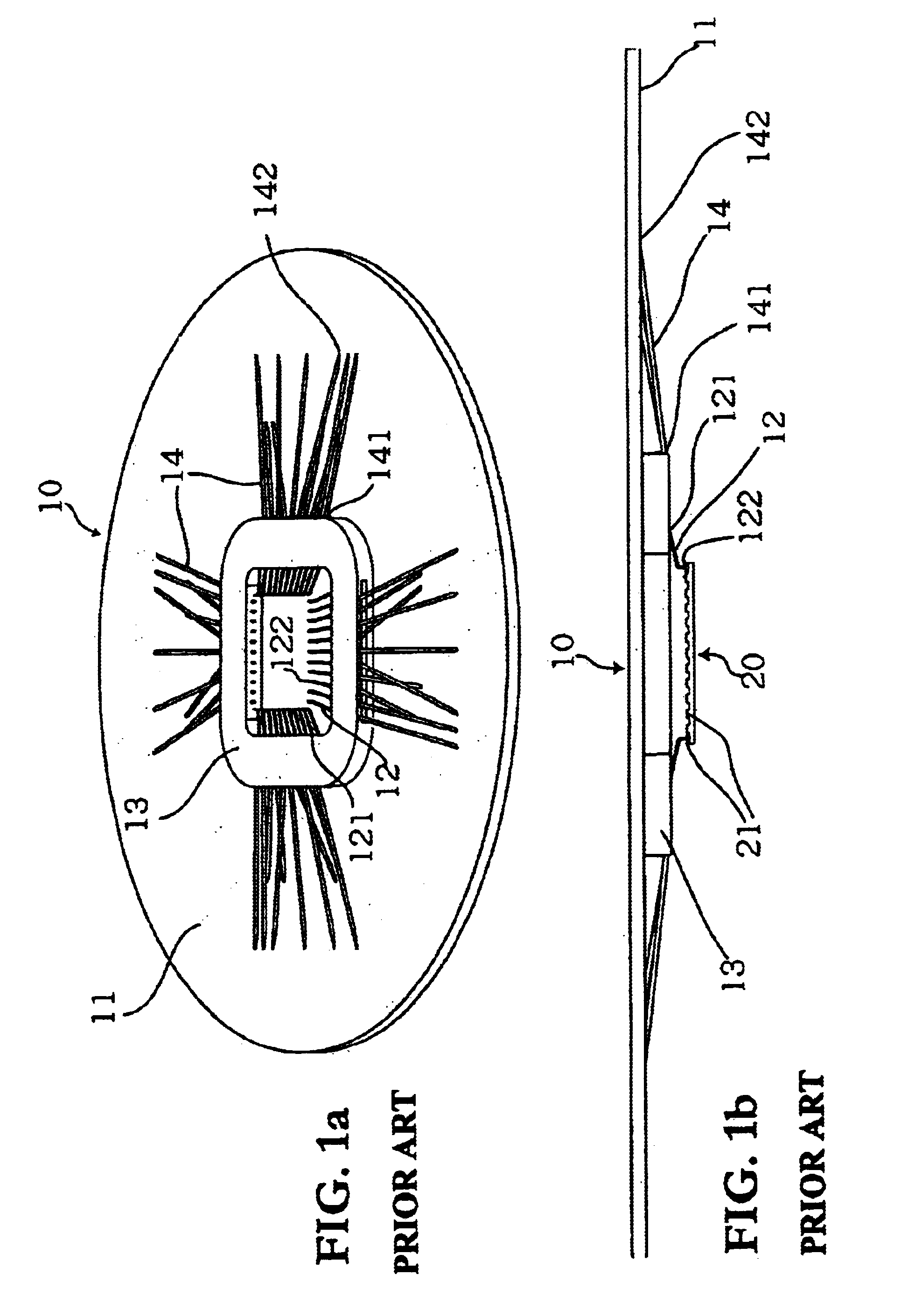
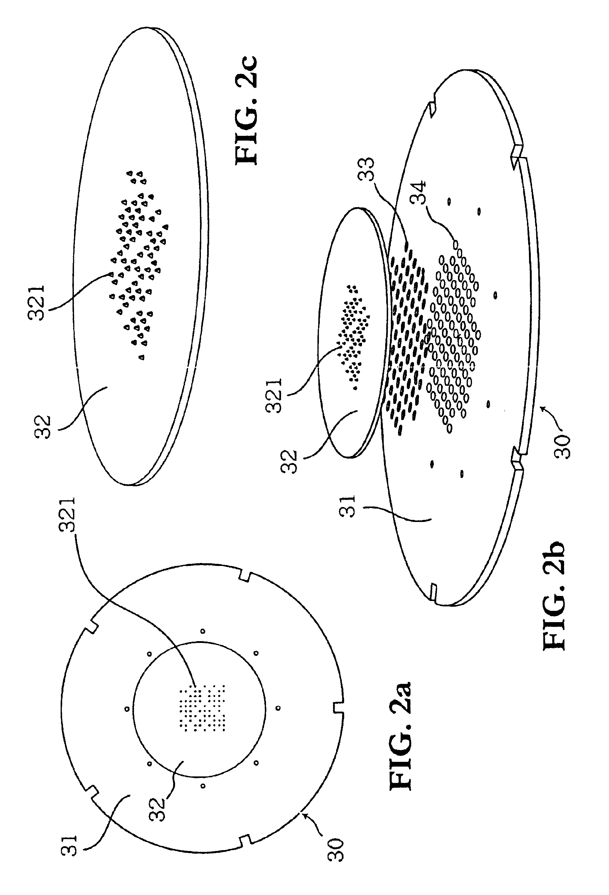
Embodiment Construction

An object of the present invention is to provide an apparatus and a method for testing dies on an integrated circuit wafer.

Another object of the present invention is to provide an apparatus and a method for testing dies on an integrated circuit wafer with more accurate results.

Still another object of the present invention is to provide an apparatus and a method for testing integrated circuit devices that are made in reduced sizes or with denser I / O terminals.

A further object of the present invention is to provide an apparatus and a method for testing integrated circuit devices that have I / O terminals not only on their circumference but also in central areas of the devices. Similarly, it is desirable for the testing apparatus and method be adapted to test devices that can be mounted on a printed circuit board using flip chip technologies.

A further object of the present invention is to provide an apparatus and a method that can test integrated circuit devices with very high frequency ...


PUM

PropertyMeasurementUnit
safety distanceaaaaaaaaaa
temperatureaaaaaaaaaa
conductiveaaaaaaaaaa

Abstract

A vertical probe card for testing electronic devices includes a multi-layer ceramic substrate mounted on a printed circuit board. The multi-layer ceramic substrate provides a plurality of vertical probes arranged in a planar array and formed on the surface of the multi-layer ceramic substrate by micro-fabrication technology. The method of using the vertical probe card includes disposing a device to be tested under the card, aligning the card's probes with the I / O terminals of the device, and contacting the device with the card's ceramic substrate so that all of the contact portions of the I / O terminals are contacted and deformed by the probes. The relative positions of the electronic device and the apparatus are maintained while Automatic Test Equipment tests the device.

Description

This application claims priority from Taiwanese patent application 91101112, filed Jan. 24, 2002, which application is incorporated by reference in its entirety.BACKGROUND1. Field of the InventionThe present invention relates to an apparatus and a method for testing electronic devices, especially for testing one or more dies on a integrated circuit (IC) wafer.2. Description of the Related ArtTesting IC characteristics and the reliability of ICs is indispensable to the semiconductor industry. As IC manufacturing technology advances, ICs perform better and are able to work at higher frequencies with even smaller die sizes. The technology and equipment for IC testing needs to advance correspondingly. The number and density of the probes on a testing probe card should conform with those of the I / O terminals of the ICs to be tested. All the lines and leads from the probes to the Automatic Test Equipment (ATE) that generates and processes testing signals should be able to work at higher f...

Claims


Application Information

Patent Timeline
Patent Type & Authority Patents(United States)
IPC IPC(8): G01R1/073
CPCG01R1/07342
Inventor CHEN, HSING-HSINHSU, HOWARD
Owner SCS HIGHTECH
Why Eureka
Try Eureka