Method and apparatus for high speed IC test interface

Inactive Publication Date: 2005-02-22
CREDENCE SYSTEMS
View PDF6 Cites 37 Cited by
  • Summary
  • Abstract
  • Description
  • Claims
  • Application Information

AI Technical Summary

Benefits of technology

The present disclosure is directed to a testing method and circuits to test high speed communication devices on otherwise conventional (lower speed) Automatic Test Equipment (ATE), e.g., testing very high speed (2.5 Gbps and higher operating speed) integrated circuits operating at speeds higher than conventional testing equipment. The circuit fans out the data stream from the output pins or ports of the Device Under Test (DUT) to multiple ATE tester channels. The testing method and design also allow for the injectio

Problems solved by technology

The challenge in testing high-speed electronic circuit interfaces has been present for several years.
In communication devices and applications for high speed networking devices called serializers and de-serializers (SERDES), under-sampling can be harmful in the sense that it masks test failures.
Under-sampling could potentially mask such errors if it occurs outside of the sampling window.
However, there are several disadvantages associated with this method.
First, the test data received is restricted to what has been transmitted, which complicates test pattern generation and restricts fault coverage for DUT manufacturing defects.
This restricts ability of the testing equipment to characterize the clock recovery mechanism and to inject jitter in order to test the response of the system.
Moreover, in non-SER

Method used


Image

  • Method and apparatus for high speed IC test interface
  • Method and apparatus for high speed IC test interface
  • Method and apparatus for high speed IC test interface

Examples


Embodiment Construction

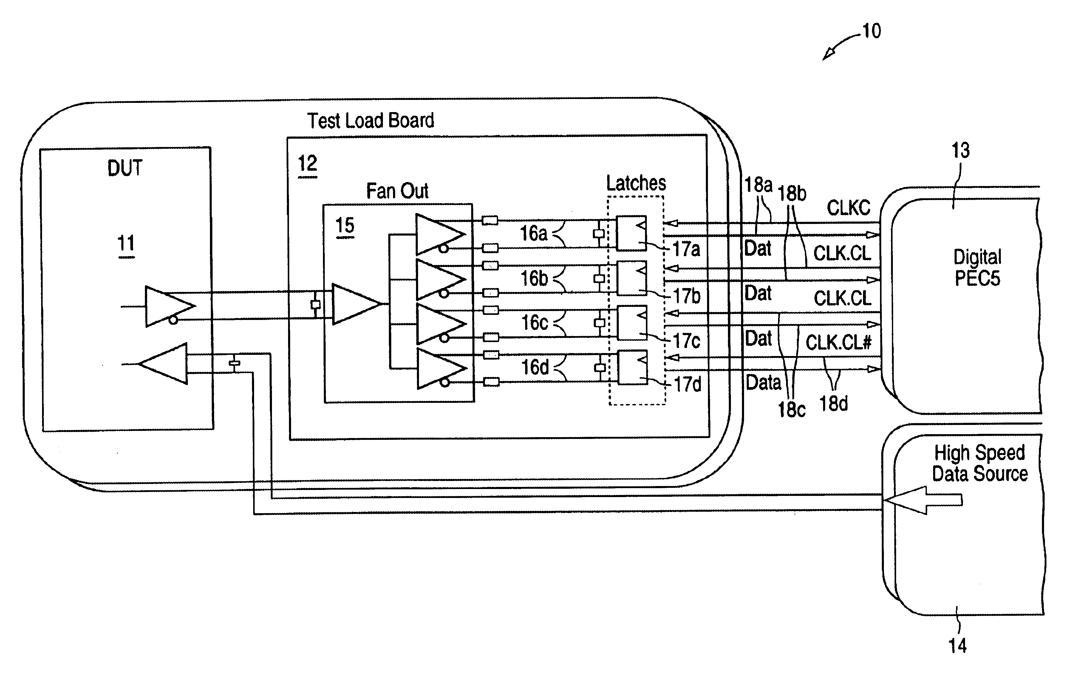
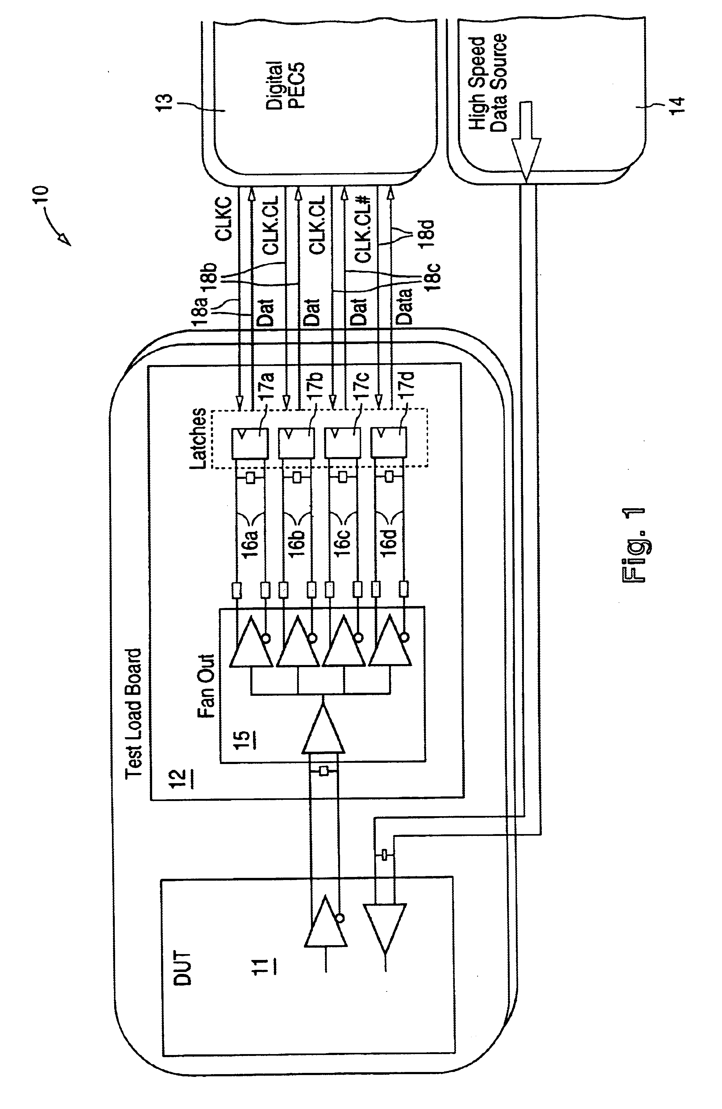
FIG. 1 provides a high-level depiction of major components of the present testing system 10. The data rate of test data from the DUT 11 is several times higher than the base data rate of the conventional portions of test system 10. An interface circuit 12 is coupled between the DUT 11 and the tester 13 which includes Digital Pin Electronics (PEC) and software operating the system 10. DUT 11 accepts input from a high speed data source 14, such as a High Speed Clock Card (HSCC), which can be considered a sub-component of the tester 13. Interface circuit 12 branches the data stream from DUT 11 into multiple tester resources in tester 13. These tester resources, when used in concert, can accept the very high data rates of interest. Assuming a case of data output at a 3.2 Gbps rate from the DUT 11, four tester resources (channels) operating at 800 Mbps each would be required to accommodate the DUT rate (4×800 Mbps=3.2 Gbps). System 10 also handles the bandwidth limitation of the tester c...


PUM


Abstract

A testing method and circuit used to test high-speed communication devices on Automatic Test Equipment—ATE. The method and circuit provide a solution to testing very high speed (2.5 Gbps and above) integrated circuits. The circuit fans out the data streams from the output of the Device Under Test (DUT) to multiple tester channels which under-sample the streams. The testing method and circuit also allow for the injection of jitter into to the DUT at the output of the DUT. The skipping of data bits inherent in multi-pass testing is avoided by duplicating the tester resources to achieve effective real-time capture (saving test time and improving Bit Error Rate). Moreover the circuit synchronizes different DUTs with the timing of ATE hardware independent of DUT output data. Also, a calibration method is used compensate for differing trace lengths and propagation delay characteristics of test circuit components.

Description

FIELD OF THE INVENTIONThis disclosure relates to testing techniques and circuits for testing high-speed communication devices on Automatic Test Equipment (ATE).RELATED ARTThe challenge in testing high-speed electronic circuit interfaces has been present for several years. In most cases in the past the data rates were ten times the standard rate of the available ATE equipment. Some approaches have used multiplexing to provide a high speed data sources to Devices Under Test (DUTs) typically receiving data input at high speeds. See, for example, “Multiplexing Test System Channels for data rates Above 1 Gbps” by David Keezer—Univ. of South Florida, 1990 International Test Conference, Paper 18.3.Other data handling solutions previously contemplated are tailored toward SONET and Datacom Ics such as that presented in the paper “Frequency enhancement of digital VLSI systems,” by Leslie Ackner & Mark Barber—AT&T Bell Labs, Allentown Pa., 1990 International Test Conference, Paper 22.1. At the...

Claims


Application Information

Patent Timeline
IPC IPC(8): G01R31/28G01R31/3193G01R31/319G01R31/317
CPCG01R31/2884G01R31/31709G01R31/31937G01R31/3171G01R31/31905G01R31/31926G01R31/28
Inventor DALAL, WAJIHSHIMANOUCHI, MASASHIGLENN, ROBERT J.WEST, BURNELL G.
Owner CREDENCE SYSTEMS
Why Eureka
Try Eureka