Auto-recovery wafer testing apparatus and wafer testing method

a testing apparatus and wafer technology, applied in automated testing systems, semiconductor/solid-state device testing/measurement, instruments, etc., can solve problems such as increased manufacturing costs, increased production efficiency, and accidental system interruptions, and achieve the effect of saving testing time and production costs

Active Publication Date: 2005-10-20
POWERCHIP SEMICON MFG CORP +1
View PDF2 Cites 4 Cited by
  • Summary
  • Abstract
  • Description
  • Claims
  • Application Information

AI Technical Summary

Benefits of technology

[0009] In view of the above, the present invention is to provide an auto-recovery wafer testing method, whereby, whenever a testing is accidentally interrupted and resumption of the testing process becomes necessary, a testing unit is able to return to the testing position prior to the interruption of the system for saving testing time and production costs.

Problems solved by technology

However, during the conventional processes of the foregoing wafer probing, laser trimming or final test step, interruptions may occur accidentally due to a breakdown of the testing apparatus (e.g., probing card and laser trimmer) or other unforeseeable causes.
When that happens, the testing data for the chips that have been tested on a wafer will be lost upon the interruption of the system.
Such repetitive testing processes due to data loss may cause damages on the chips through multiple testing processes, and the resetting of the testing apparatus will also lengthen the entire trimming process to cause the increase of the manufacturing cost and decrease of the production efficiency.

Method used


Image

  • Auto-recovery wafer testing apparatus and wafer testing method
  • Auto-recovery wafer testing apparatus and wafer testing method
  • Auto-recovery wafer testing apparatus and wafer testing method

Examples


Embodiment Construction

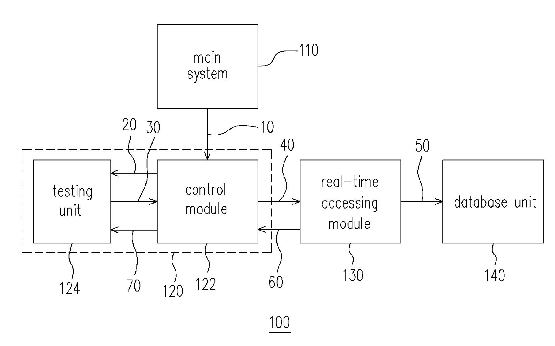
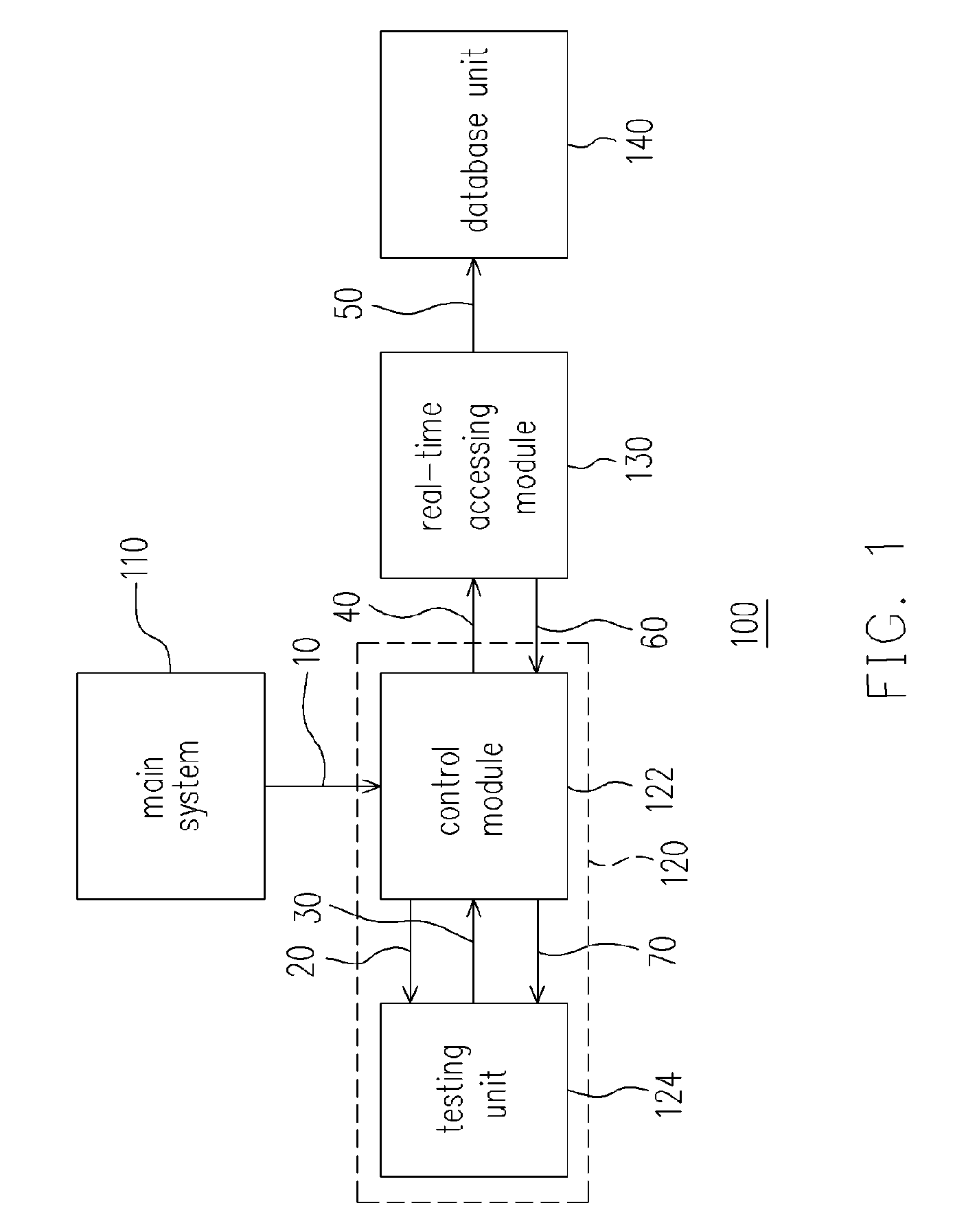
[0022] The auto-recovery wafer testing apparatus and wafer testing method of this invention are suitable to, for example, perform wafer probing, laser trimming or final test on a plurality of chips on a wafer in a semiconductor manufacturing process.

[0023]FIG. 1 is a block diagram schematically illustrating an auto-recovery wafer testing apparatus according to the present invention. The wafer testing apparatus 100 includes a main system 110, a tester 120, a real-time accessing module130, and a database unit 140. The main system 110 is, for example, a manufacturing execution system (MES) for controlling the overall wafer testing process that involves manufacturing parameters such as wafer transferring, manufacture category, wafer batch numbers, wafer serial number, manufacture time.

[0024] Referring further to FIG. 1, the tester 120 includes, for example, a control module 122 and a testing apparatus 124, wherein the testing unit 124 is, for example, a wafer prober for wafer probing,...


PUM


Abstract

Auto-recovery wafer testing apparatus and wafer testing method are provided. The wafer testing apparatus includes a main system, a tester and a real-time accessing module. The main system controls the process of the wafer testing. The tester is electrically coupled to the main system for receiving commands from the main system to perform testing on a plurality of chips sequentially and output the testing data correspondingly. The real-time accessing module is electrically coupled to the tester for simultaneously accessing the testing data. In an event when the testing is accidentally interrupted, the tester can produce auto-recovery data according to the testing data saved in the real-time accessing module, and continue testing, based on the auto-recovery data, from the chip being last but incompletely tested. The use of the wafer testing apparatus and method can save testing time and enhance the production efficiency.

Description

CROSS-REFERENCE TO RELATED APPLICATION [0001] This application is a divisional of a prior application Ser. No. 10 / 710,670, filed Jul. 28, 2004, which claims the priority benefit of Taiwan application serial no. 93110813, filed Apr. 19, 2004.BACKGROUND OF THE INVENTION [0002] 1. Field of the Invention [0003] The present invention generally relates to a wafer testing apparatus and wafer testing method, and more particularly relates to an auto-recovery wafer testing apparatus and wafer testing method. [0004] 2. Description of the Related Art [0005] In today's society of information explosion, the market for the use of multimedia expends dramatically, which further induces the development of electronic devices moving towards digitalization, network accessibility, regional connection, and personalization. Responding to the demands, it is necessary for integrated circuits devices to meet the requirements of high-speed treatment, multi-functionality, integration, miniaturization and cost e...

Claims


Application Information

Patent Timeline
Patent Type & Authority Applications(United States)
IPC IPC(8): G01R31/26G01R31/28H01L21/00H01L21/66
CPCH01L21/67288G01R31/2834
Inventor WU, CHIOU-PINGLIN, HSIU-MIN
Owner POWERCHIP SEMICON MFG CORP
Why Eureka
Try Eureka