

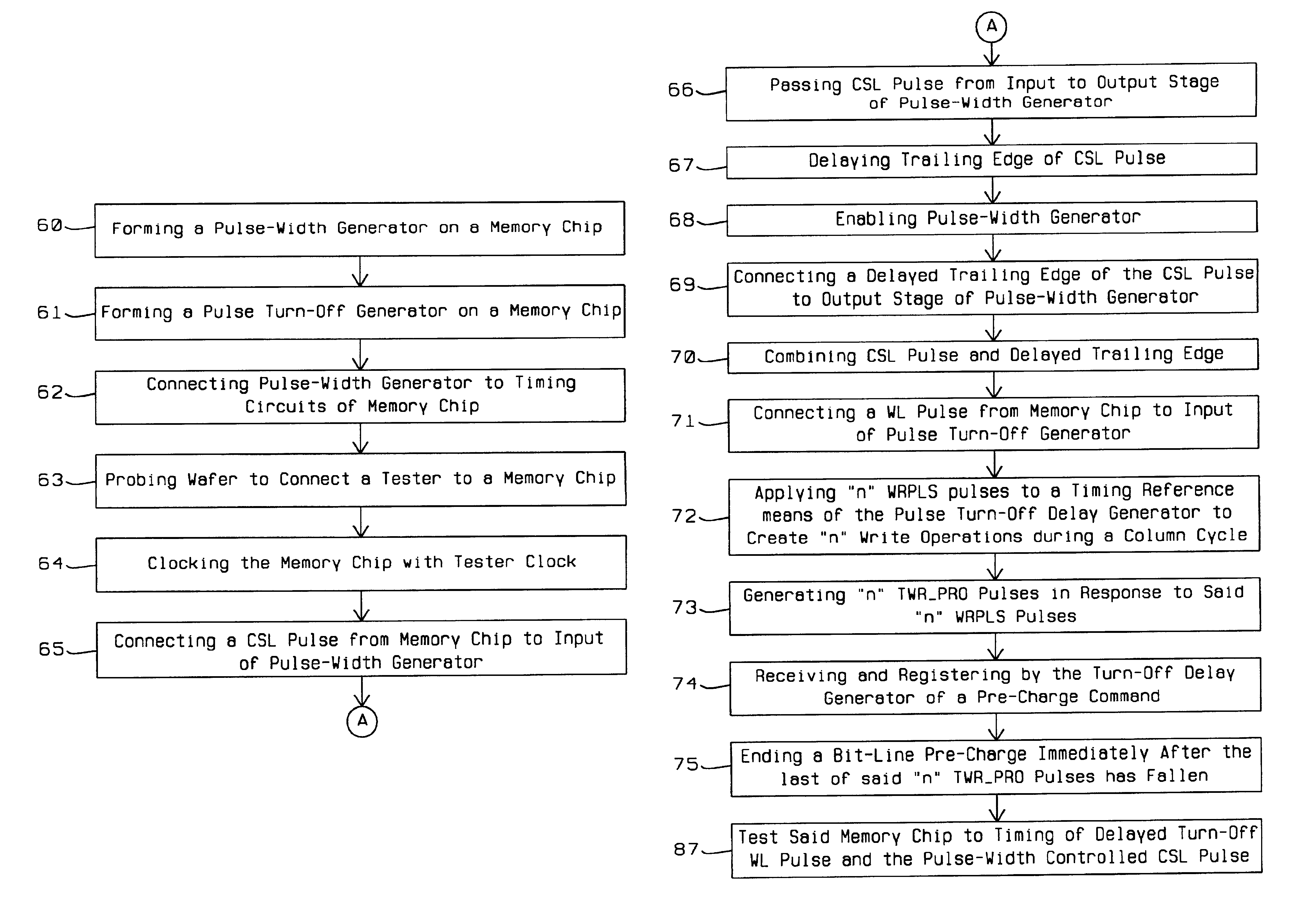
Variable self-time scheme for write recovery by low speed tester
a write recovery and variable time scheme technology, applied in the field of integrated circuit device fabrication, can solve the problems of increased data storage capability, more expensive methods of memory device testing, etc., and achieve the effect of saving test tim
- Summary
- Abstract
- Description
- Claims
- Application Information
AI Technical Summary
Benefits of technology
Problems solved by technology
Method used
Image

Examples
Embodiment Construction
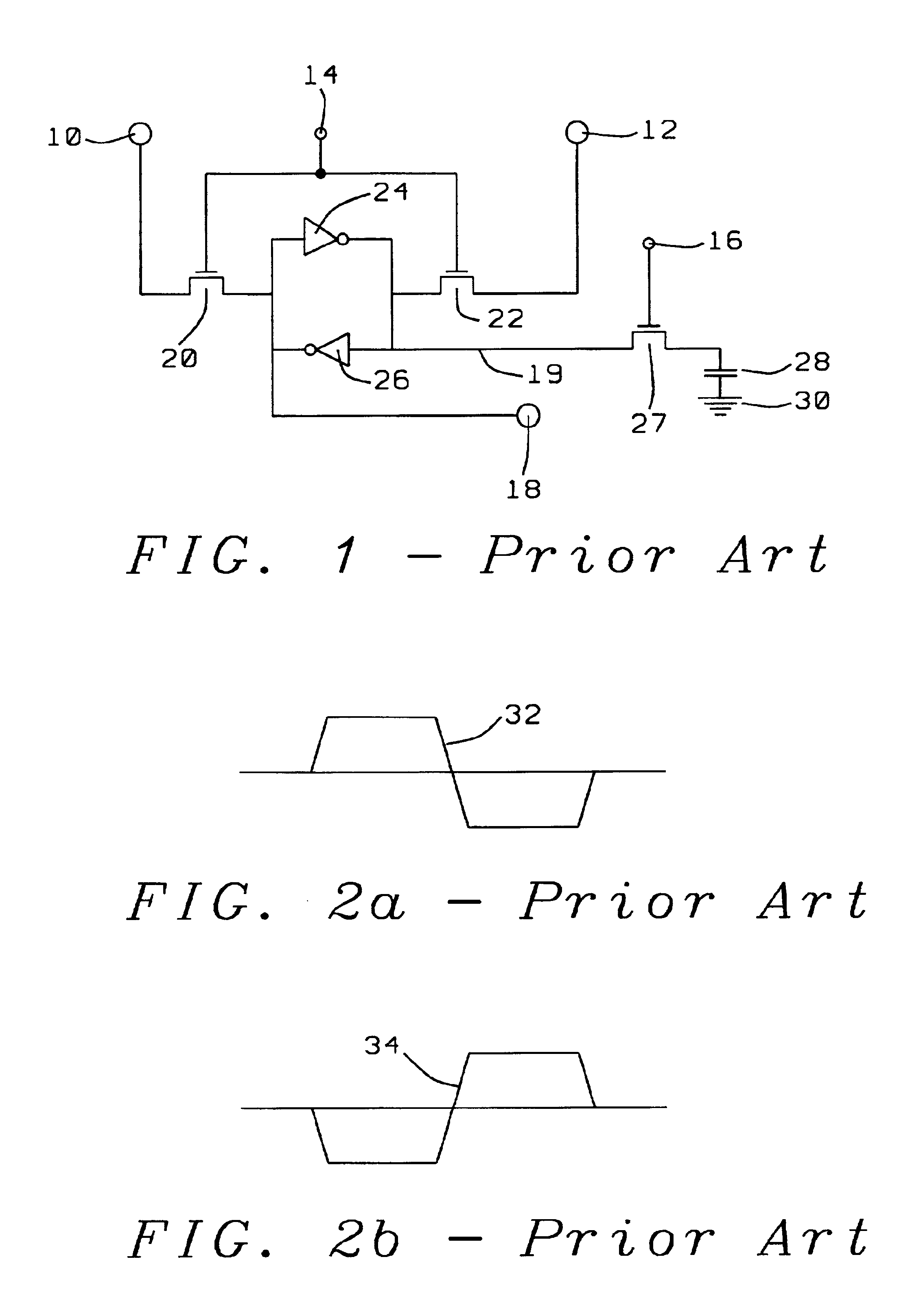
[0023]In test mode, several registers are available that can be used to control the on-width of the CSL and WL pulses. In this manner the on-width of the CSL pulse can be adjusted by for instance 4 or 5 nanoseconds. Equally valid, the WL fall time, which is timed with respect to the CMD rise time, can be adjusted. These adjustments are applied to a conventional DRAM cell sense amplifier, the operation of which will first be highlighted using FIG. 1.
[0024]Highlighted in FIG. 1 are the following components, which collectively form a standard DRAM bit line sense amplifier driving a DRAM cell:[0025]10, a first data line input DLB[0026]12, a second data line input DL[0027]14, a column select input CSL[0028]16, a word line input WL[0029]18, a first bit line output BLB[0030]19, a second bit line output BL, connected to the source / drain of transistor 27[0031]20 and 22, CSL transistors[0032]24 and 26, inverters for DLB and DL input data lines respectively[0033]27, the word line select transi...
PUM
 Abstract
Description
Claims
Application Information