Laser-induced critical parameter analysis of CMOS devices

a technology of critical parameter analysis and cmos, which is applied in the field of semiconductor device testing, can solve the problems of shortening the test cycle, increasing and disturbing the circuitry of the light energy dut, so as to improve the visual resolution of the test, shorten the test cycle, and increase the frequency with which the failure occurs

Active Publication Date: 2006-03-30
TWITTER INC
View PDF11 Cites 38 Cited by
  • Summary
  • Abstract
  • Description
  • Claims
  • Application Information

AI Technical Summary

Benefits of technology

[0012] According to an aspect of the invention, the ATE can be configured to “short-cycle” the test up to the point of failure detection, when a failure is detected. This effectively improves the test's visual “resolution”. “Short-cycling” involves resetting the test back to its starting point whenever a failure is detected. In the present context, a “fa

Problems solved by technology

This light energy “disturbs” circuitry of the DUT wherever it strikes.
By resetting the test back to its starting point when a failure is detected, test s

Method used


Image

  • Laser-induced critical parameter analysis of CMOS devices
  • Laser-induced critical parameter analysis of CMOS devices
  • Laser-induced critical parameter analysis of CMOS devices

Examples


Embodiment Construction

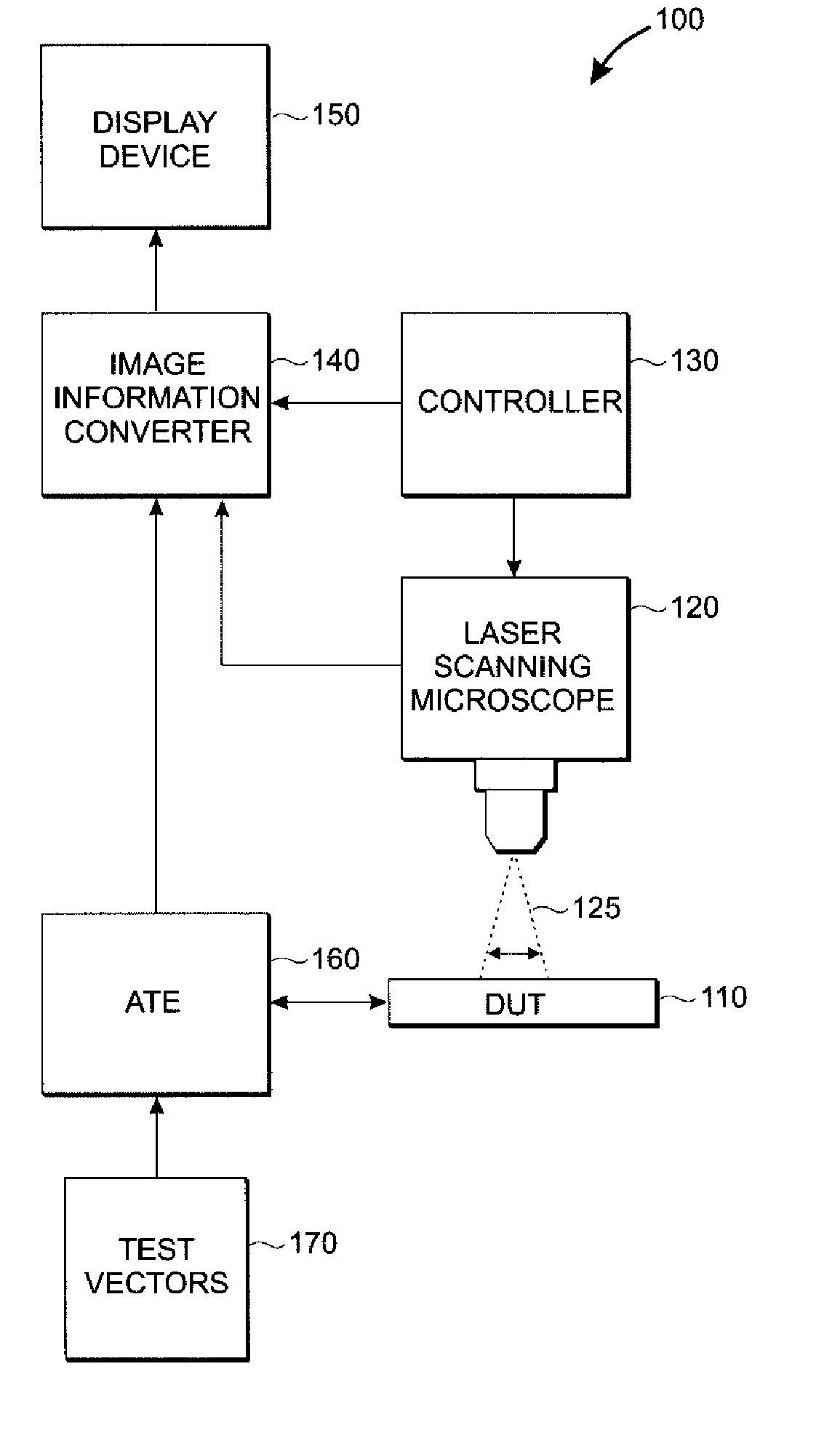
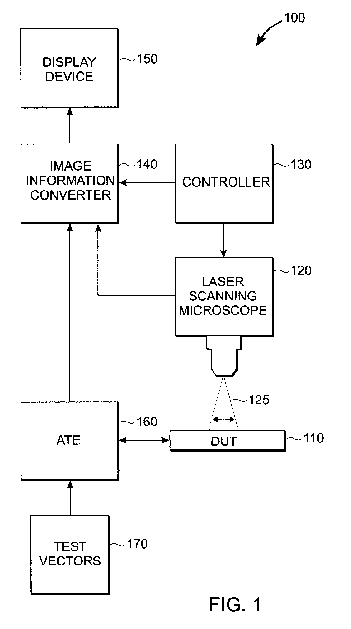
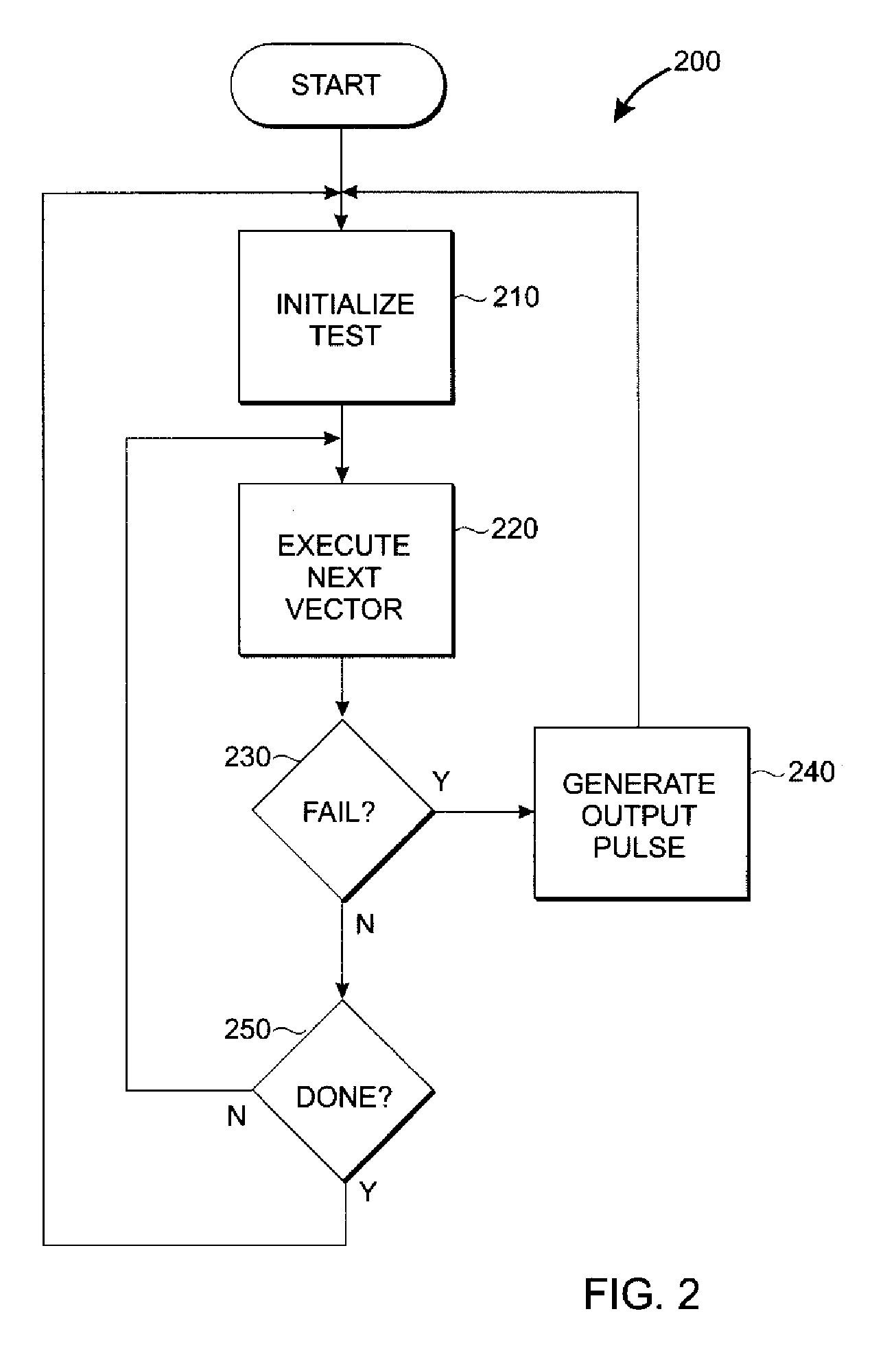
[0016] The present inventive technique provides Critical Parameter Analysis of complex semiconductor devices by combining the capabilities of automated test equipment (ATE) and optical beam microscopes (e.g., Laser Scanning Microscope or LSM). The ATE provides stimulus for the semiconductor device (a Device Under Test or DUT, e.g., a complex CMOS integrated circuit), while the Laser Scanning Microscope (or similar device) scans the semiconductor device, simultaneously producing a viewable image thereof and imparting photonic (light) energy to selected elements thereof as the scanning beam passes thereover. Whenever the ATE detects a device failure (i.e., when the DUT fails to generate an expected response to ATE stimulus) the ATE generates an output pulse. This output pulse is provided as an input to the LSM video display system in much the same manner described hereinabove with respect to Cole '305, Cole '183 and Koyama to produce a visible spot overlaying the viewable image that i...


PUM


Abstract

A technique is described for performing critical parameter analysis (CPA) of a semiconductor device (DUT) by combining the capabilities of conventional automated test equipment (ATE) with a focused optical beam scanning device such as a laser scanning microscope (LSM). The DUT is provided with a fixture such that it can be simultaneously scanned by the LSM or a similar device and exercised by the ATE. The ATE is used to determine pass/fail boundaries of operation of the DUT. Repeatable pass/fail limits (for timing, levels, etc.) are determined utilizing standard test patterns and methodologies. The ATE vector pattern(s) can then be programmed to “loop” the test under a known passing or failing state. When light energy from the LSM scanning beam sufficiently disturbs the DUT to produce a transition (i.e., to push the device outside of its critical parameter limits), this transition is indicated on the displayed image of the DUT, indicating to the user which elements of the DUT were implicated in the transition.

Description

BACKGROUND OF INVENTION [0001] The present invention relates to semiconductor device testing, and more particularly to detecting failures and failure mechanisms in semiconductor integrated circuitry, especially CMOS (Complementary Metal-Oxide-Semiconductor) integrated circuitry. [0002] As semiconductor devices (e.g., CMOS integrated circuits) become increasingly complex, it becomes increasingly difficult, and increasingly important, to identify elements of those devices that affect common failure modes and “critical parameters” of the device. Typically, critical parameters are “spec sheet” performance limits that dictate whether a completed device meets or fails to meet its target specifications. Examples of such limits are critical setup times, hold times, min / max propagation delays, etc. Other examples include min / max voltage levels at a given drive current, min / max slew rates or rise / fall times (usually determined by comparing a voltage against predetermined threshold levels befo...

Claims


Application Information

Patent Timeline
IPC IPC(8): G01R31/302
CPCG01R31/311
Inventor MCGINNIS, PATRICK J.SYLVESTRI, JOHN D.
Owner TWITTER INC
Why Eureka
Try Eureka