Eureka AIR delivers breakthrough ideas for toughest innovation challenges, trusted by R&D personnel around the world.

Clock frequency divider circuit

Active Publication Date: 2006-05-25
SONY SEMICON SOLUTIONS CORP
View PDF4 Cites 1 Cited by
  • Summary
  • Abstract
  • Description
  • Claims
  • Application Information

AI Technical Summary

Benefits of technology

[0009] It is accordingly desirable to make it possible to divide the frequency of a clock signal with an arbitrary frequency dividing ratio, and obtain a clock signal of a desired frequency.
[0012] According to a second embodiment of the present invention, there is provided a clock frequency divider circuit for dividing frequency of a predetermined input clock signal with a frequency dividing ratio obtained by dividing a numerator setting value by a denominator setting value. The clock frequency divider circuit includes adding means for adding a previous result of addition to one of a difference between the numerator setting value and the denominator setting value and the numerator setting value; storing means for storing a result of addition by the adding means in synchronism with the input clock signal, and supplying the stored result of addition as the previous result of addition to the adding means; retaining means for retaining a most significant bit of the result of addition stored by the storing means in synchronism with the input clock signal; and logical product generating means for generating a logical product of the most significant bit of the result of addition retained by the retaining means and the input clock signal, and outputting the logical product as an output clock signal. In an initial stage in which the result of addition is not obtained, the storing means supplies a predetermined initial value as the previous result of addition to the adding means. The adding means selects one of the difference between the numerator setting value and the denominator setting value and the numerator setting value on a basis of a value of the most significant bit of the previous result of addition, adds the previous result of addition to a result of the selection, and supplies a result of the addition to the storing means. It is thereby possible to divide the frequency of an input clock signal with an arbitrary frequency dividing ratio, and obtain an output clock signal of a desired frequency.
[0014] According to a third embodiment of the present invention, there is provided a clock frequency divider circuit for dividing frequency of a predetermined input clock signal with a frequency dividing ratio obtained by dividing a numerator setting value by a denominator setting value. The clock frequency divider circuit includes a subtracter for performing a predetermined subtraction process; a register for storing a first output value from the subtracter in synchronism with the input clock signal, and outputting a second output value corresponding to the first output value in synchronism with the input clock signal; a selector for selecting one of the denominator setting value and a value “0” according to a third output value corresponding to a value of a most significant digit when the second output value from the register is represented in binary notation, and outputting a result of the selection as a fourth output value; an adder for adding the numerator setting value to the second output value outputted from the register, and outputting a fifth output value corresponding to a result of the addition; a latch for retaining the third output value corresponding to the value of the most significant digit of the second output value outputted from the register in synchronism with the clock signal; and a logical product circuit for calculating a logical product of a sixth output value outputted from the latch and the clock signal, and outputting a result of the calculation as an output clock signal. In the subtracter subtracts the fourth output value outputted from the selector from the fifth output value outputted from the adder, and outputs the first output value corresponding to a result of the subtraction. It is thereby possible to divide the frequency of an input clock signal with an arbitrary frequency dividing ratio, and obtain an output clock signal of a desired frequency.
[0016] According to a fourth embodiment of the present invention, there is provided a clock frequency divider circuit for dividing frequency of a predetermined input clock signal with a frequency dividing ratio obtained by dividing a numerator setting value by a denominator setting value. The clock frequency divider circuit includes: an adder for performing a predetermined addition process; a register for storing a first output value from the adder in synchronism with the input clock signal, and outputting a second output value corresponding to the first output value in synchronism with the input clock signal; a selector for selecting one of the numerator setting value and a value corresponding to a result of subtraction of the denominator setting value from the numerator setting value according to a third output value corresponding to a value of a most significant digit when the second output value from the register is represented in binary notation, and outputting a result of the selection as a fourth output value; a latch for retaining the third output value corresponding to the value of the most significant digit of the second output value outputted from the register in synchronism with the clock signal; and a logical product circuit for calculating a logical product of a sixth output value outputted from the latch and the clock signal, and outputting a result of the calculation as an output clock signal. In the adder adds the fourth output value outputted from the selector to the second output value outputted from the register, and outputs the first output value corresponding to a result of the addition. It is thereby possible to divide the frequency of an input clock signal with an arbitrary frequency dividing ratio, and obtain an output clock signal of a desired frequency.
[0018] The present invention can produce an excellent effect of making it possible to divide the frequency of a clock signal with an arbitrary frequency dividing ratio, and generate a clock signal of an arbitrary frequency.

Problems solved by technology

However, a conventional frequency divider circuit using a scale-of-D counter has a disadvantage of being able to perform only 1 / D (D is a natural number) frequency division.
In addition, the clock signal generating circuit according to Patent Literature 1 has a problem in that the number of bits of the adder and the D-type flip-flop circuit limits the frequency dividing ratio of the clock signal generating circuit to the frequency dividing ratio as expressed by the above equation.

Method used


Image

  • Clock frequency divider circuit
  • Clock frequency divider circuit
  • Clock frequency divider circuit

Examples


first embodiment

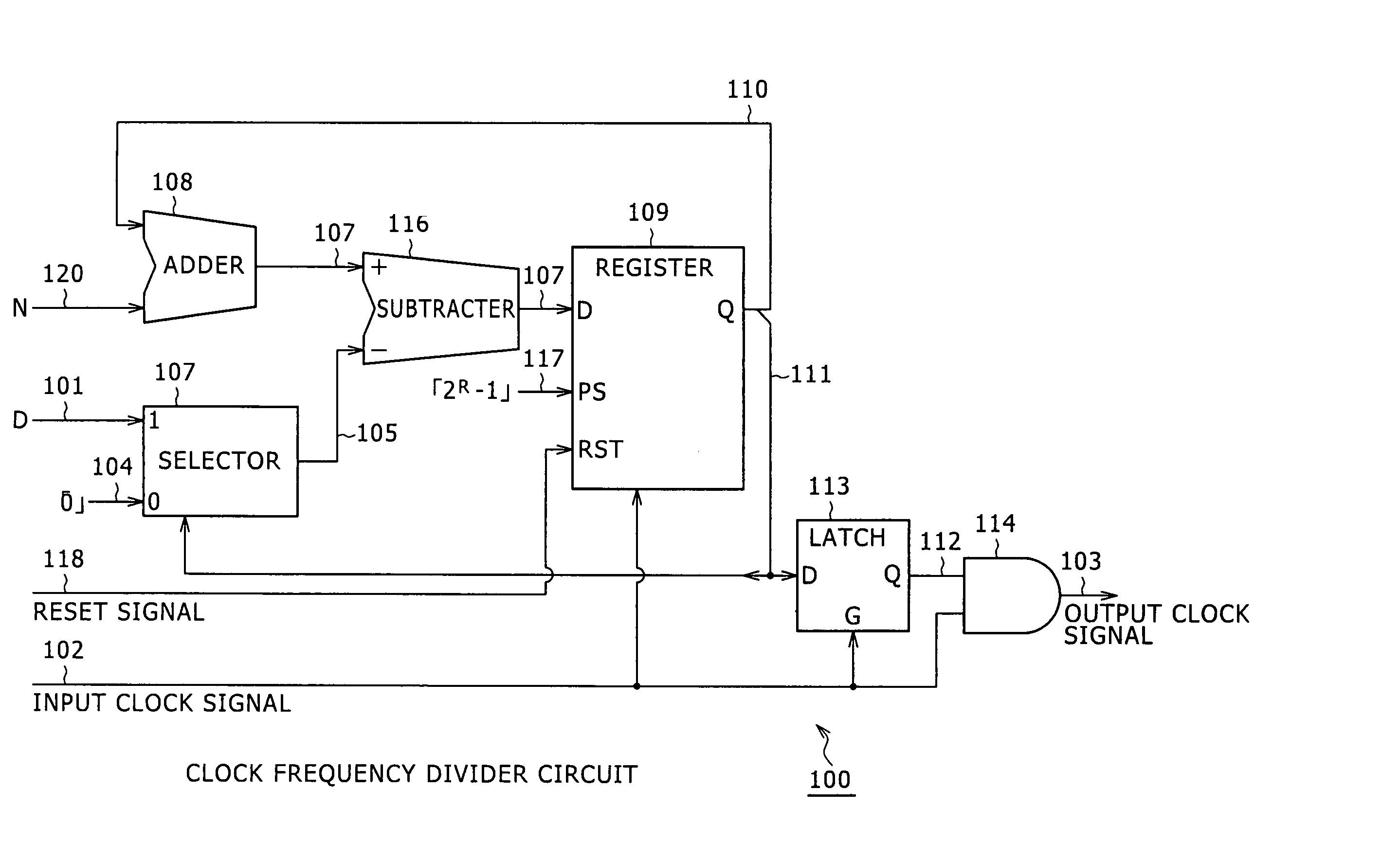
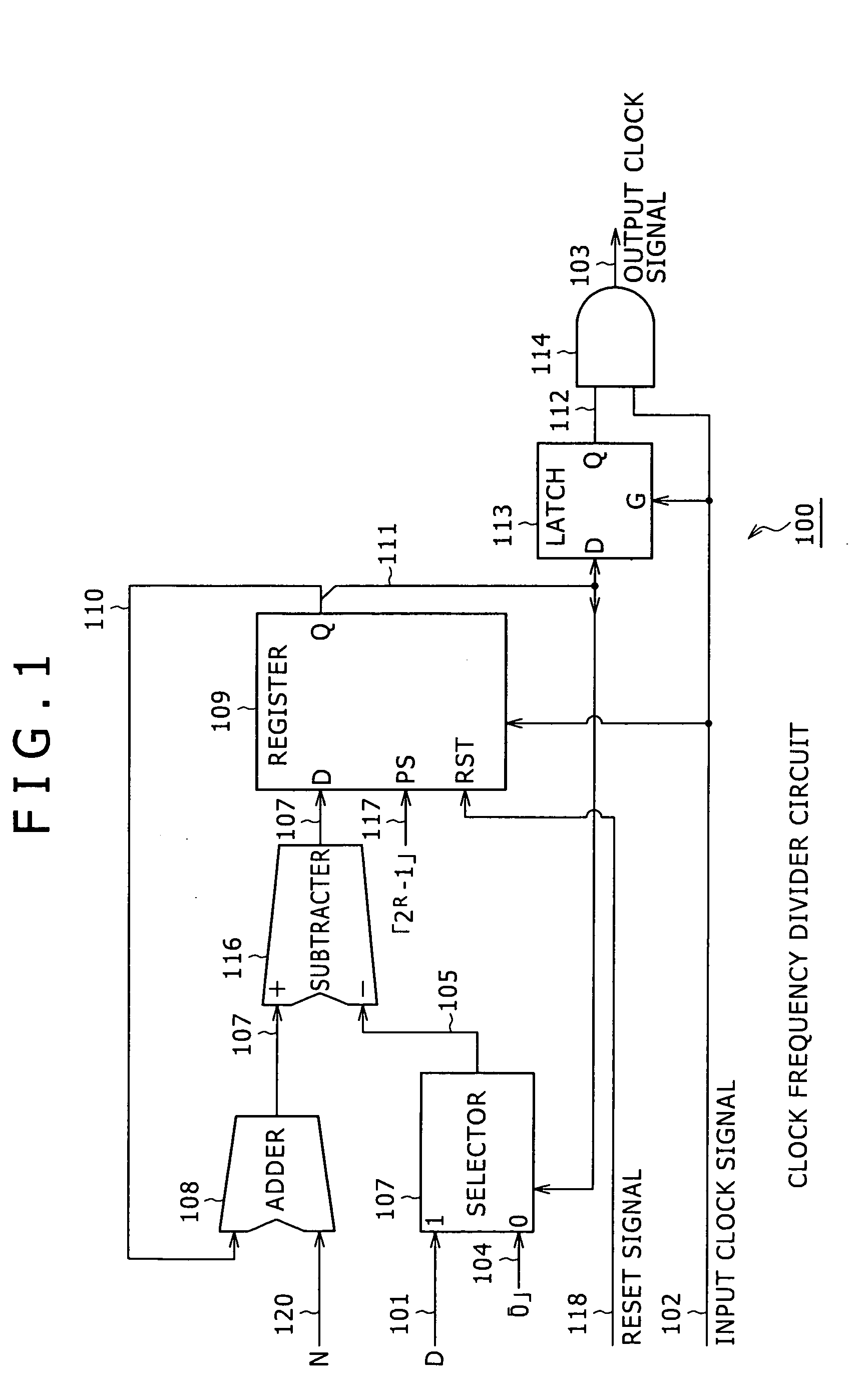
[0024]FIG. 1 is a diagram showing an example of configuration of a clock frequency divider circuit 100 according to the present invention. This clock frequency divider circuit 100 subjects an input clock signal 102 to N / D frequency division, where N is a numerator setting value of a frequency dividing ratio (N / D), and D is a denominator setting value of the frequency dividing ratio. However, it is assumed that the numerator setting value N and the denominator setting value D of the frequency dividing ratio are each an arbitrary natural number, and each satisfy a condition (N≦D) and a condition (D!=0).

[0025] The clock frequency divider circuit 100 includes a selector 107, an adder 108, a subtracter 116, a register 109, a latch 113, and a logical product circuit 114.

[0026] The selector 107 is supplied with an input signal 101 corresponding to the denominator setting value D of the frequency dividing ratio, an input signal 104 corresponding to a value “0,” and an output signal 111 cor...

second embodiment

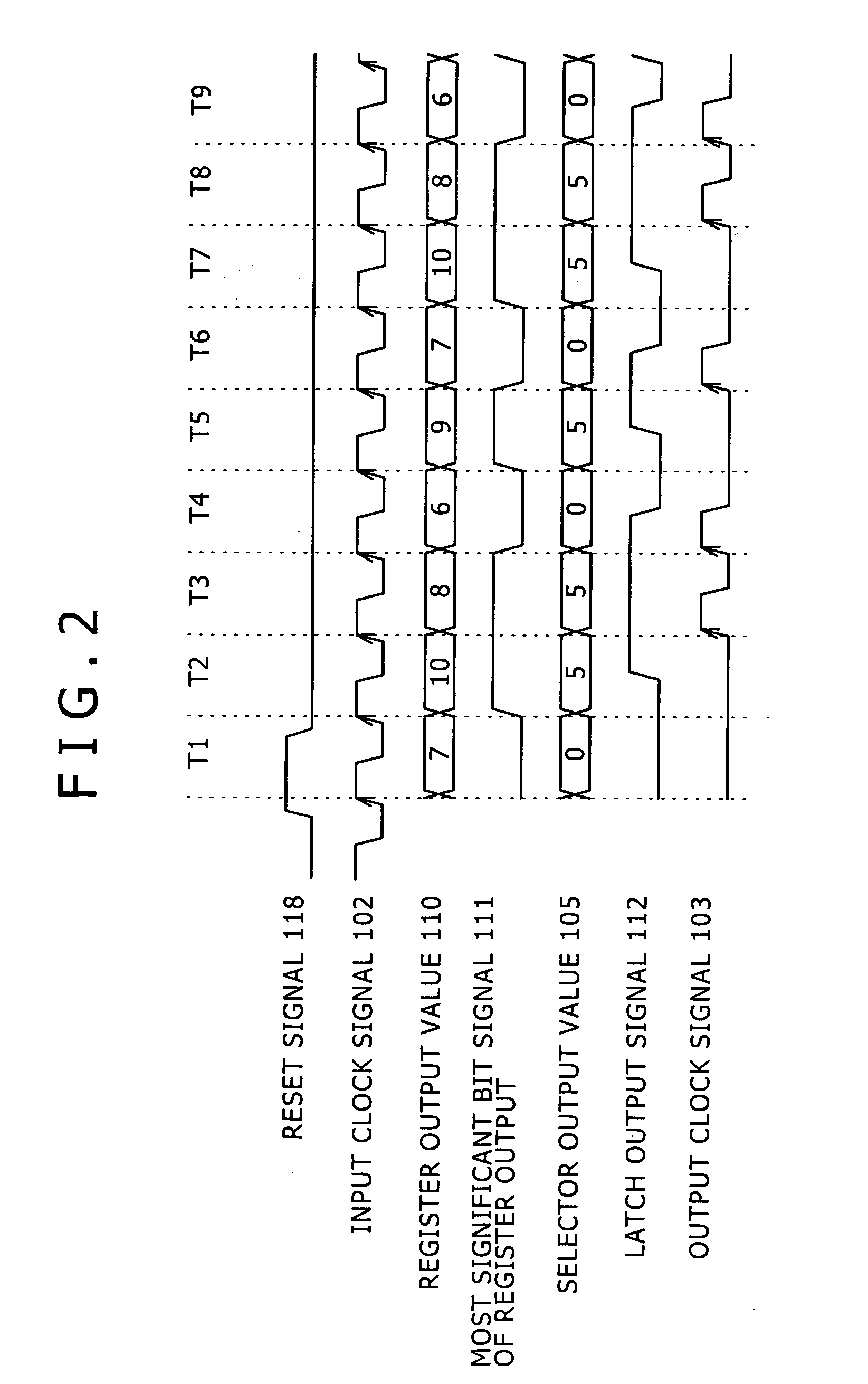
[0098] The operation of the clock frequency divider circuit 200 according to the present invention will next be described concretely with reference to FIG. 3 and FIG. 4. FIG. 4 is a timing chart showing operation when it is assumed that N=3 and D=5 and N / D (=3 / 5) frequency division is performed in the clock frequency divider circuit 200 of FIG. 3. Suppose in the following that a period from a rising edge of the input clock signal 202 to a next rising edge of the input clock signal 202 is one cycle, and that cycles are described as T1, T2, T3, . . . . In this case, from the above Equation (1), R is 3 (=ceil(log(5) / log(2)).

[0099] First, when the reset signal 218 is set to a high level, an initial value “7” (=2R−1) is set in the register 209 by the input signal 217. In this case, from the above Equation (1), R is 3.

[0100] Next, in cycle T1 from a rising edge of the input clock signal 202 to a next rising edge of the input clock signal 202, the register 209 outputs the register output ...


PUM


Abstract

A clock frequency divider circuit including: a storing section for storing an input signal in synchronism with an input clock signal; a supplying section for supplying, as the input signal, one of a first value obtained by adding a value stored by the storing section to a numerator setting value and a second value obtained by subtracting a denominator setting value from the first value; a retaining section for retaining a most significant bit of the value stored by the storing section in synchronism with the input clock signal; and a logical product generating section for generating a logical product of a value retained by the retaining section and the input clock signal, and outputting the logical product as an output clock signal; wherein the supplying section supplies one of the first value and the second value as the input signal on a basis of the most significant bit of the value stored by the storing section.

Description

CROSS REFERENCES TO RELATED APPLICATIONS [0001] The present invention contains subject matter related to Japanese Patent Application JP 2004-339353 filed in Japanese Patent Office on Nov. 24, 2004, the entire contents of which being incorporated herein by reference. BACKGROUND OF THE INVENTION [0002] The present invention relates to a clock frequency divider circuit, and particularly to a clock frequency divider circuit that divides the frequency of an input clock signal, and generates a clock signal with an arbitrary frequency dividing ratio. [0003] Conventionally, each element in a semiconductor integrated circuit is basically controlled with a clock signal as a basis, and operating speed of each element is determined by the clock signal. A quartz oscillator is generally used as an oscillating source for generating a clock signal supplied to a semiconductor integrated circuit, because of stability and accuracy of the quartz oscillator. [0004] Since clock signals of various frequen...

Claims


Application Information

Patent Timeline
IPC IPC(8): H03K23/00
CPCH03K23/52H03K21/00G06F1/08
Inventor HASEGAWA, KOICHI
Owner SONY SEMICON SOLUTIONS CORP
Why Eureka
Eureka Blog
Learn More