Antenna array of printed circuit board

a printed circuit board and antenna array technology, applied in the field of antenna arrays, can solve the problems of interference of signals between these two antennas, reducing the space reserved for installing antennas in such wireless network cards, and restricting the position, so as to increase the bandwidth

Active Publication Date: 2006-05-25
ALPHA NETWORKS INC
View PDF2 Cites 20 Cited by
  • Summary
  • Abstract
  • Description
  • Claims
  • Application Information

AI Technical Summary

Benefits of technology

[0013] A further objective of the present invention is to extend a broadband plane on at least one external edge of the antenna unit to increase the bandwidth, so that a

Problems solved by technology

Therefore, the space reserved for installing an antenna in such wireless network card also becomes smaller.
Further, the internal components of the wireless network card also occupy certain spaces.
These factors definitely will restrict the position for installing the antenna in a design for wireless network cards.
Since the size of such wireless network card for the USB interface is getting smaller and smaller in these years, the distance between any two antennas installed in the wireless network card with the USB interface is becoming closer and closer and thus causing an interference of signals between these two antennas and an isolation problem between the antennas.
In general, the installation position of such chip antenna usually cannot be designed according to the best conditions recommended by the numeri

Method used


Image

  • Antenna array of printed circuit board
  • Antenna array of printed circuit board
  • Antenna array of printed circuit board

Examples


Embodiment Construction

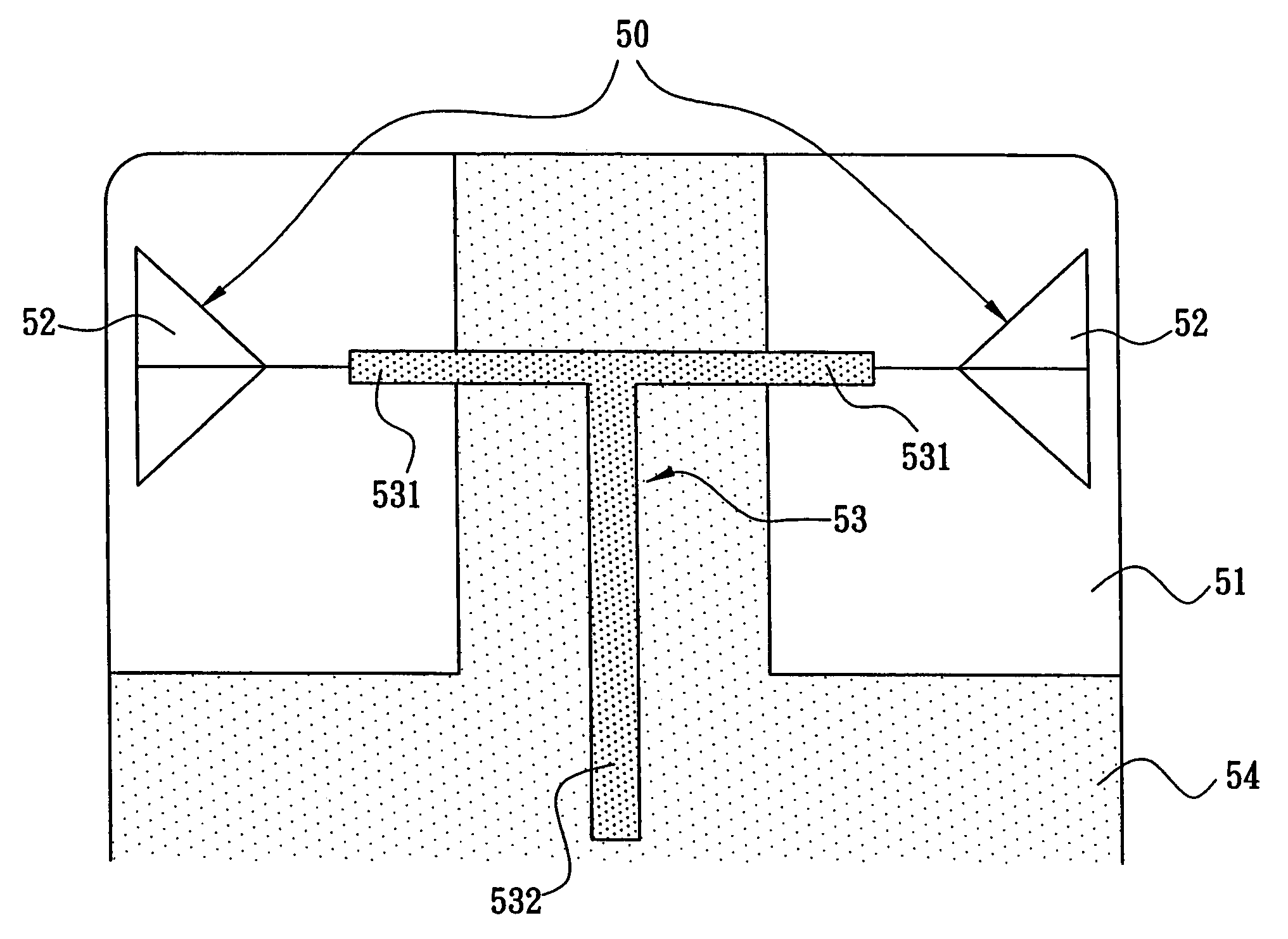
[0027] Please refer to FIG. 5 for an antenna array 50 of a printed circuit board 51. When the antenna array 50 is fabricated on a mini printed circuit board 51 of a wireless network card with a USB, the manufacturing technology for printed circuit boards 51 uses a microstrip mode to install the antenna array 50 onto one side of the printed circuit board 51. The antenna array 50 comprises two antenna units 50, and one end proximate to the antenna unit 52 is coupled separately to two symmetric ends 531 of a T-shape microstrip circuit 53 on a printed circuit board 51, and the asymmetric end 532 on the T-shape microstrip circuit 53 is coupled to a transmit circuit (not shown in the figure) on the wireless network card with a USB interface and acts as a feeding end of the antenna array 50, so that the transmit circuit on the wireless network card with a USB interface can feed signals to the two antenna units 52 through the feeding end. A grounding metal surface 54 is fabricated on the ot...


PUM


Abstract

The present invention discloses an antenna array installed on a printed circuit board, which comprises two antenna units, each being a microstrip directly installed on two symmetric ends of a T-shape microstrip on a printed circuit board and an asymmetric end of the T-shape microstrip circuit being a feeding end feeding signals simultaneously to the two antenna units. A grounding metal surface is fabricated on the other side of the printed circuit board at a position other than the antenna unit, and keeps a specific distance from at least one corresponding edge of the antenna unit. Since the antenna units are symmetric in shape and have the same feeding end, the radiation direction thereof is shifted towards the two symmetric edges to broaden the range of the use of two symmetric edges.

Description

FIELD OF THE INVENTION [0001] The present invention relates to an antenna, more particularly to an antenna array installed on a printed circuit board and comprising two antenna symmetric in shape and fed with signals via the same feeding end. Therefore, the radiation direction of the antenna array may be shifted towards the two symmetric edges to broaden the range of the use of two symmetric edges. BACKGROUND OF THE INVENTION [0002] In recent years, the market demand for mobile communications products increases drastically, and thus wireless communications are developed more quickly. Manufacturers tend to design the wireless network cards, particularly the mini wireless card designed for the USB interface smaller and smaller. Therefore, the space reserved for installing an antenna in such wireless network card also becomes smaller. Further, the internal components of the wireless network card also occupy certain spaces. These factors definitely will restrict the position for install...

Claims


Application Information

Patent Timeline
IPC IPC(8): H01Q1/38
CPCH01Q1/38H01Q9/30H01Q9/40H01Q21/061
Inventor YEH, MING-HAO
Owner ALPHA NETWORKS INC
Why Eureka
Try Eureka