Mounting structure, electro-optical device, and electronic apparatus

Active Publication Date: 2006-05-25
TCL CHINA STAR OPTOELECTRONICS TECH CO LTD
View PDF9 Cites 39 Cited by
  • Summary
  • Abstract
  • Description
  • Claims
  • Application Information

AI Technical Summary

Benefits of technology

[0008] An advantage of the invention is that it provides a mounting structure capable of protecting wiring lines on a flexible substrate, an electro-optical device including the mounting structure, and an electronic apparatus including the electro-optical device.
[0009] According to an aspect of the invention, an electro-optical device includes: a first substrate having an end edge; a second substrate that has an edge crossing the end edge and a plurality of first wiring lines crossing the end edge, the second substrate having flexibility and being connected to the first substrate so as to overlap the end edge; and first reinforcing members provided on the second substrate so as to cross the end edge, in a region between the plurality of first wiring lines and a portion where the end edge and the edge cross each other.
[0010] Here, the first wiring lines are, for example, signal wiring lines, and the first reinforcing members are signal wiring lines or insulating members. In addition, the second substrate is referred to as a flexible substrate, for example.
[0011] In accordance with the invention, even though an external force is applied to the second substrate having flexibility, the first reinforcing members are provided between the plurality of wiring lines and the portion, where the end edge of the first substrate and the edge of the second substrate cross each othe

Problems solved by technology

However, in a case in which only the dummy wiring lines are provided on the bending portion of the flexible substrate, when an external force is applied to the flexible substrate, the flexible substrate and the wiring lines are broken at the portion (end edge) where the flexible substrate comes in contact with the substrate of the liquid crystal panel and the frame, because the substrate of the liquid crystal panel and the frame are hard.
In addition, in the above-described technique, dummy wiring lines are not p

Method used


Image

  • Mounting structure, electro-optical device, and electronic apparatus
  • Mounting structure, electro-optical device, and electronic apparatus
  • Mounting structure, electro-optical device, and electronic apparatus

Examples


Example

First Embodiment

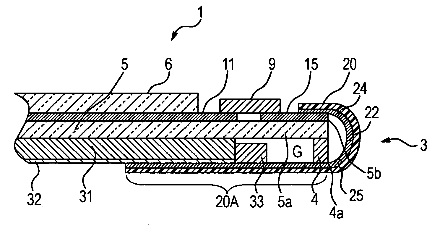
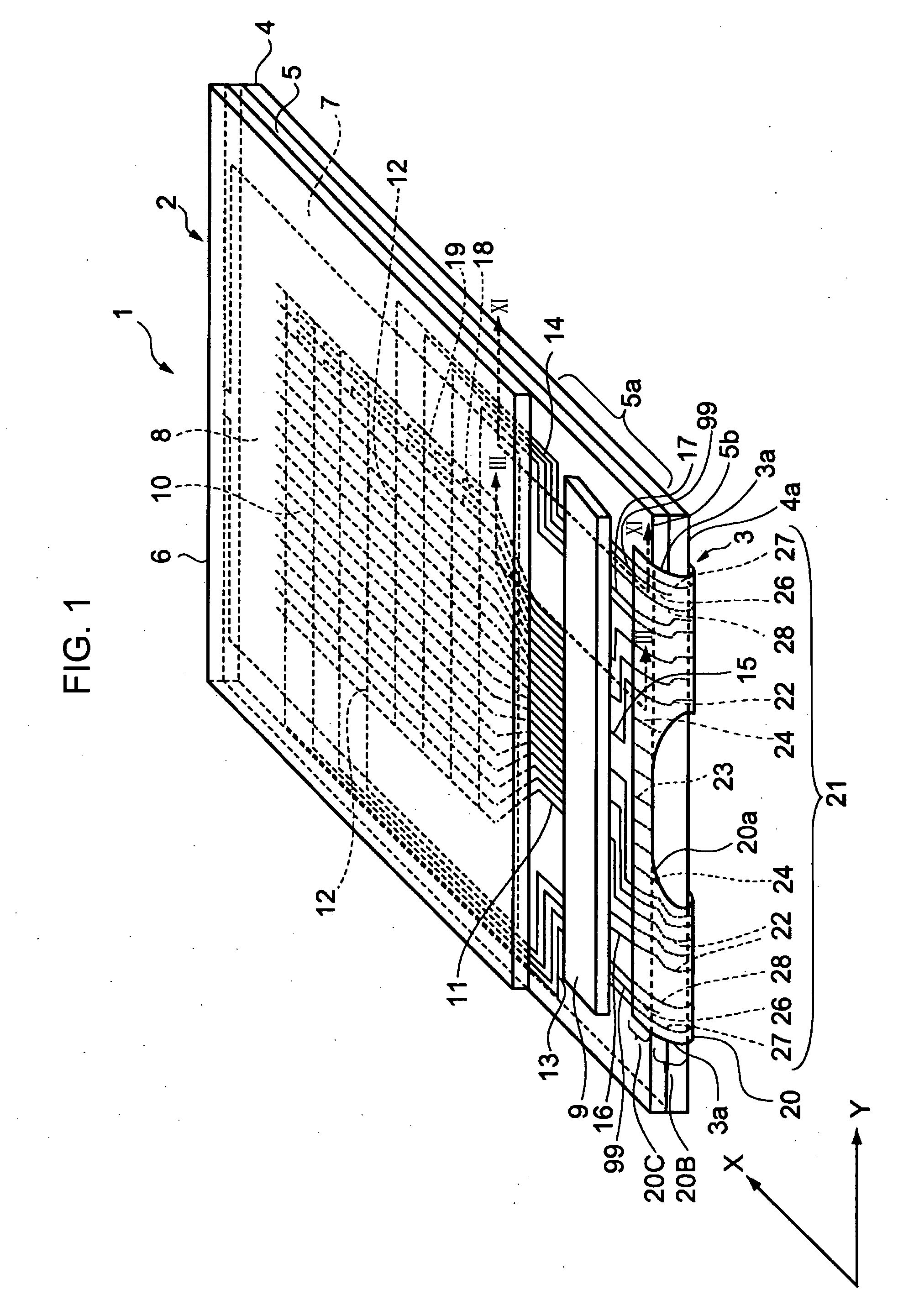
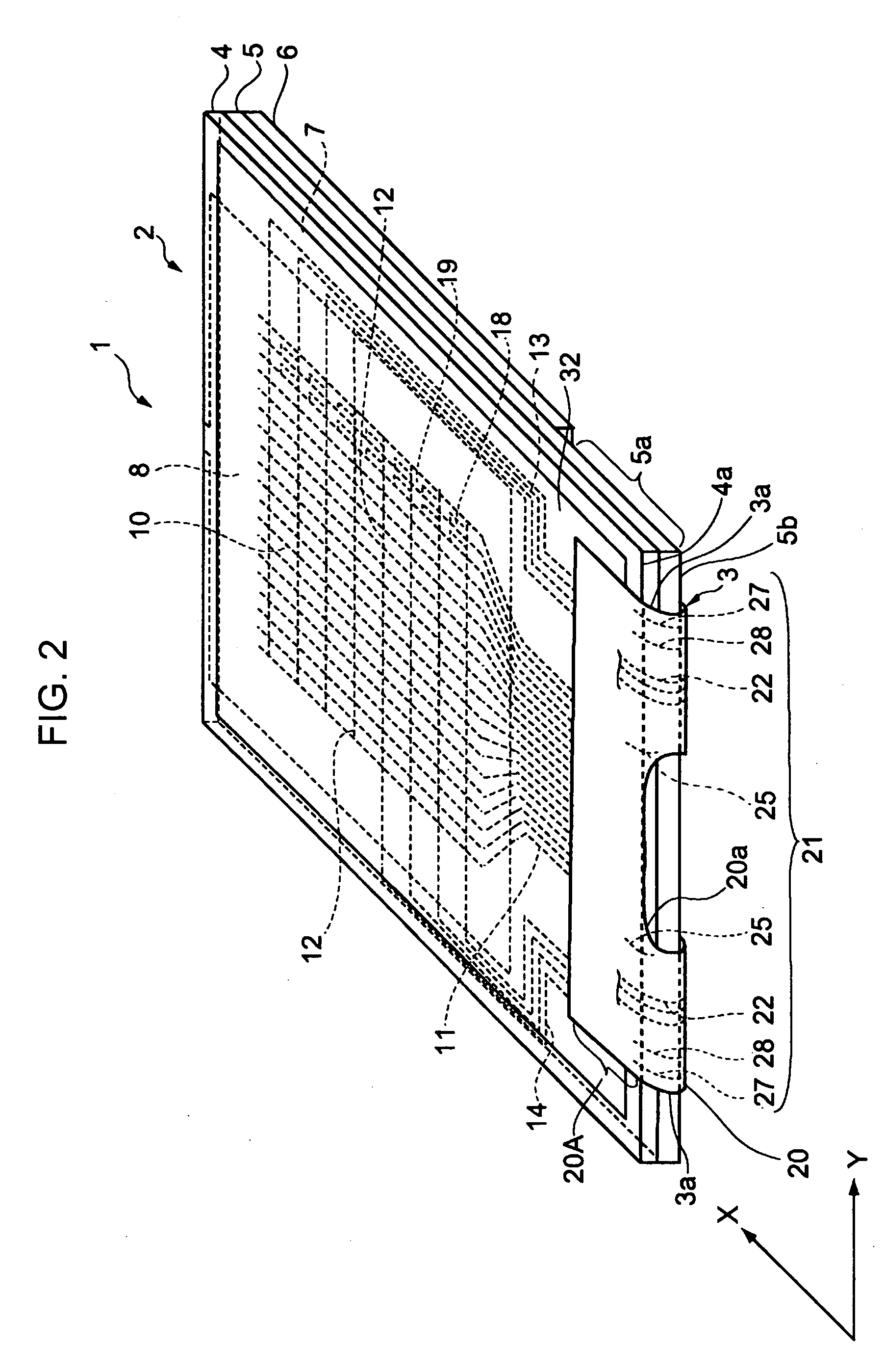
[0046]FIG. 1 is a schematic perspective view illustrating a liquid crystal display device of the first embodiment according to the invention. FIG. 2 is a schematic perspective view illustrating the liquid crystal display device, seen from the bottom surface. FIG. 3 is a cross-sectional view illustrating the liquid crystal display device shown in FIG. 1 taken along the line III-III.

[0047] The liquid crystal display device 1 of the present embodiment is provided with a liquid crystal panel 2, a circuit board 3 serving as a second substrate connected to the liquid crystal panel 2, and a frame 4 serving as a frame body which supports the liquid crystal panel 2. Moreover, other mechanisms to be described below, if necessary, are attached to the liquid crystal display device 1.

[0048] The liquid crystal panel 2 is provided with a rectangular substrate 5 serving as a first substrate, a substrate 6 provided to face the substrate 5, a sealing material 7 provided between the...

Example

Second Embodiment

[0090] Next, a liquid crystal display device of the second embodiment according to the invention will be described. Moreover, in embodiments and modifications following the present embodiment, the same numerals are attached to the same constituent members as those of the above-described embodiment, and the descriptions thereof will be omitted. Different portions will be focused to be described.

[0091]FIG. 5 is a schematic perspective view illustrating the liquid crystal display device of the second embodiment according to the invention, and FIG. 6 is a schematic plan view illustrating a FPC substrate which is used in a liquid crystal panel shown in FIG. 5.

[0092] In the liquid crystal display device 40 of the present embodiment, a circuit board 41 having a different shape from the circuit board 3 is used instead of the circuit board 3, as shown in FIG. 5.

[0093] The circuit board 41 includes a FPC substrate 42 and a wiring group 43 provided on the FPC substrate 42....

Example

Third Embodiment

[0100] Next, a liquid crystal device of the third embodiment according to the invention will be described.

[0101]FIG. 7 is a schematic plan view illustrating a circuit board which is used in the liquid crystal display device of the present embodiment.

[0102] The liquid crystal display device of the present embodiment is an example in which a circuit board 50 is used instead of the circuit board 3. On the circuit board 50, dummy wiring lines are provided to have different widths in the direction crossing the extending direction thereof.

[0103] The circuit board 50 includes a FPC substrate 51 composed of a mounting portion 51A, a bending portion 51B, and an end portion 51C, similar to the above-described embodiment. Further, the circuit board 50 includes dummy wiring lines 52, 53, 54, 55, and 56 which have different widths from the above-described wiring lines in the Y direction crossing the extending direction.

[0104] The dummy wiring line 52, which is provided in an...


PUM


Abstract

An electro-optical device includes: a first substrate having an end edge; a second substrate that has an edge crossing the end edge and a plurality of first wiring lines crossing the end edge, the second substrate having. flexibility and being connected to the first substrate so as to overlap the end edge; and first reinforcing members provided on the second substrate so as to cross the end edge, in a region between the plurality of first wiring lines and a portion where the end edge and the edge cross each other.

Description

BACKGROUND OF THE INVENTION [0001] 1. Technical Field [0002] The present invention relates to a mounting structure having a flexible substrate, to an electro-optical device including the substrate, and to an electronic apparatus having the electro-optical device. [0003] 2. Related Art [0004] In the related art, liquid crystal display devices have been used as a display device of an electronic apparatus such as a personal computer and a mobile phone. The liquid crystal display device includes a liquid crystal panel in which liquid crystal is sealed between a pair of substrates facing each other, and a flexible substrate overlapping an extending portion of one of the substrates extending from the other substrate. On the flexible substrate, wiring lines connected to electric wiring lines on the substrate of the liquid crystal panel are provided, and the flexible substrate is properly bent to be housed in a frame or the like which supports the liquid crystal panel. There is disclosed a ...

Claims


Application Information

Patent Timeline
IPC IPC(8): G02F1/1333
CPCG02F1/13452G02F2001/13456H05K1/0281H05K3/361H05K2201/09063H05K2201/09781H05K2201/2009H05K2201/056H05K2201/10128G02F1/13456G02F1/1345
Inventor MIYAGAWA, SAKIKOKOBAYASHI, SHINICHI
Owner TCL CHINA STAR OPTOELECTRONICS TECH CO LTD
Why Eureka
Try Eureka