Wide bandgap semiconductor layers on SOD structures

a semiconductor layer and sod structure technology, applied in semiconductor/solid-state device manufacturing, semiconductor devices, electrical equipment, etc., can solve the problems of limited performance and end-of-life reliability of semiconductor devices, limited maximum performance, and limited thermal energy

Inactive Publication Date: 2006-06-01
SP3 +1
View PDF7 Cites 50 Cited by
  • Summary
  • Abstract
  • Description
  • Claims
  • Application Information

AI Technical Summary

Problems solved by technology

Thus some semiconductor devices are limited in performance and end-of-life (EOL) reliability due to high device operating temperatures.
High electron mobility transistor (HEMT) structures that use compound semiconductors provide high energy efficiency, but maximum performance is limited by thermal management problems during device operation.
The critical reliability challenge is to minimize thermal energy near the transistor junction or channel.

Method used


Image

  • Wide bandgap semiconductor layers on SOD structures
  • Wide bandgap semiconductor layers on SOD structures
  • Wide bandgap semiconductor layers on SOD structures

Examples


example

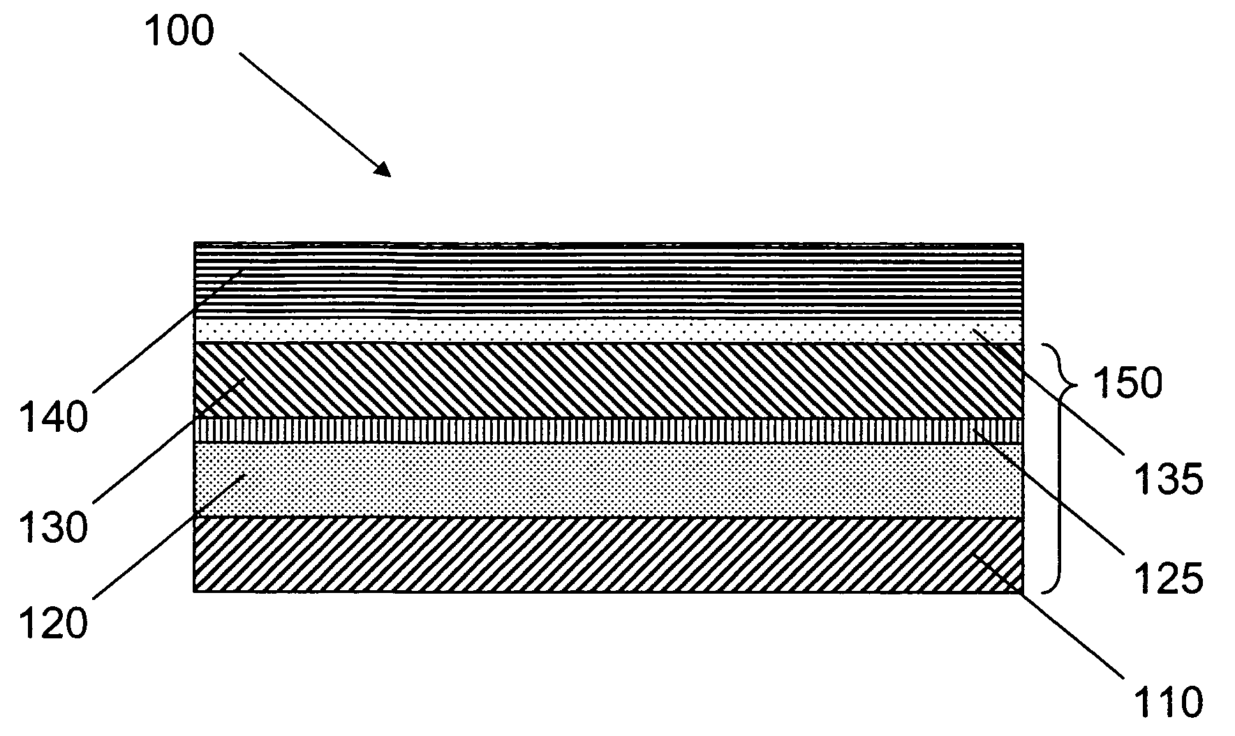
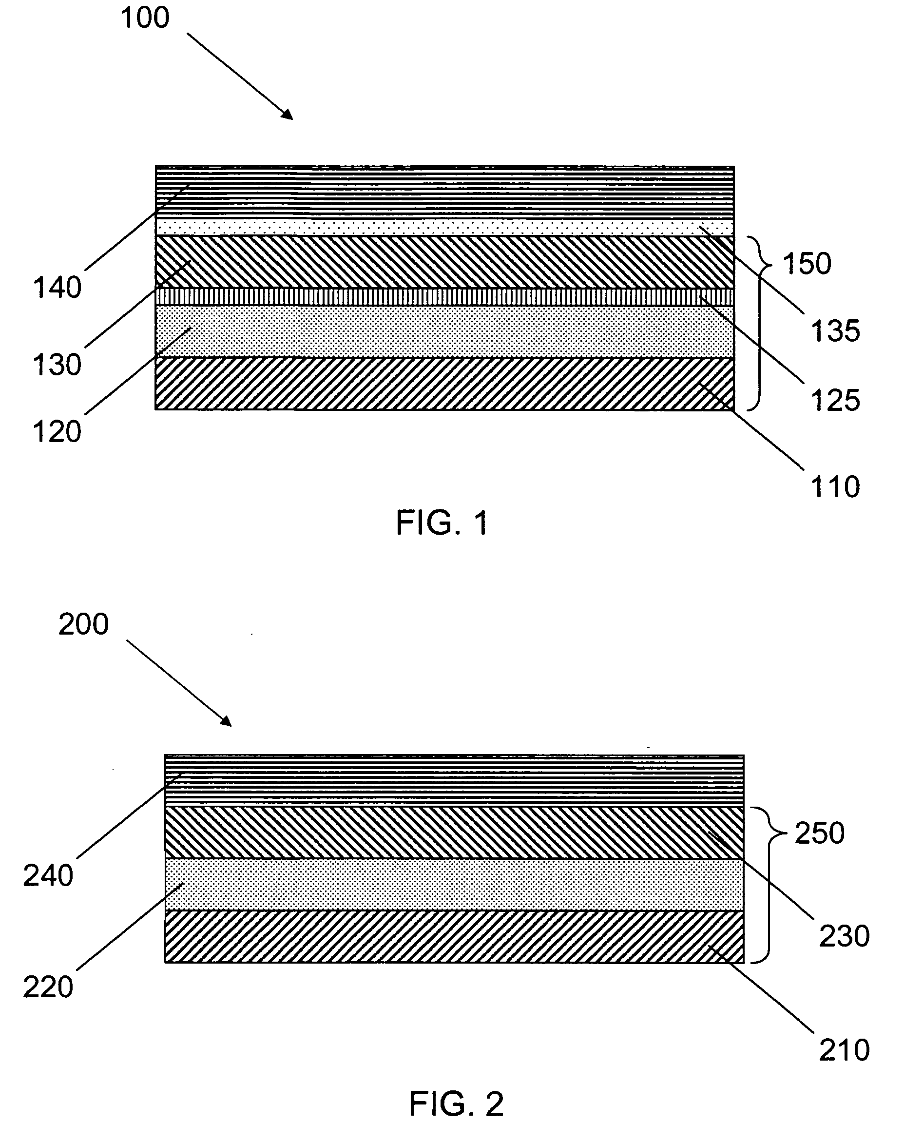
[0029] Growth of a device quality AlGaN / GaN HEMT structure on 100 mm silicon-on-diamond (SOD) substrates was performed. Growth was done on a initial SOD wafer with thin diamond and relatively thick silicon on top of the diamond. The 100 mm SOD substrate consisted of a base wafer (3-6 ohm-cm p type silicon), a diamond layer (˜3 micron), a polysilicon layer (˜23 microns) and a top silicon layer (˜15 microns of float zone (FZ) silicon [>10 kohm-cm]). Thickness values are based on interpretation of a focused ion beam (FIB) cross section of the finished wafer. The vast majority of the SOD substrate had the appearance of a typical epi-ready FZ Si wafer routinely used for growth of GaN on Si. Microscope inspection of the interior of the wafer before growth revealed a featureless surface.

[0030] The structure consisted of a (Al,Ga)N transition layer, a GaN buffer layer, a 175 Å Al0.26Ga0.74N device layer, and a ˜20 Å GaN cap layer. Growth was carried out in a vertical, cold wall, rotating...


PUM


Abstract

Multi-layered structures containing GaN on SOD (silicon / diamond / silicon) substrates are described. The unique substrate / epilayer combination can provide electronic materials suitable for high-power and opto-electronic devices without commonly observed limitations due to excess heat during device operation. The resulting devices have built-in thermal heat spreading capability that result in better performance and higher reliability.

Description

CROSS-REFERENCE TO RELATED APPLICATIONS [0001] This application claims priority to U.S. Patent Provisional Application 60 / 618,956, filed Oct. 14, 2004, which is incorporated by reference herein.STATEMENT OF GOVERNMENTAL SUPPORT [0002] The invention described and claimed herein was made in part utilizing funds supplied by the U.S. Department of Energy under Contract No. DE-AC03-76SF00098, and more recently under DE-AC02-05CH11231. The government has certain rights in this invention.BACKGROUND OF THE INVENTION [0003] Many electronic systems are being designed to accommodate high power transmitters that generate large thermal loads. Thus some semiconductor devices are limited in performance and end-of-life (EOL) reliability due to high device operating temperatures. High electron mobility transistor (HEMT) structures that use compound semiconductors provide high energy efficiency, but maximum performance is limited by thermal management problems during device operation. The critical re...

Claims


Application Information

Patent Timeline
Patent Type & Authority Applications(United States)
IPC IPC(8): H01L31/0312
CPCH01L21/02381H01L21/02439H01L21/02444H01L21/0245H01L21/02458H01L21/02502H01L21/02538H01L21/0254H01L21/0262H01L29/2003H01L29/267H01L33/641
Inventor WEBER, EICKE R.ZIMMER, JERRY W.
Owner SP3
Why Eureka
Try Eureka