

Plasma display apparatus and driving method thereof
a technology of display apparatus and plasma, which is applied in the direction of color television details, television systems, instruments, etc., can solve the problems of reducing the contrast value of the darkroom, reducing the contrast ratio, and increasing the amount of light emission, so as to reduce the substrate wall charge, widen the operation margin, and reduce the effect of darkroom contras
- Summary
- Abstract
- Description
- Claims
- Application Information
AI Technical Summary
Benefits of technology
Problems solved by technology
Method used
Image

Examples
first embodiment
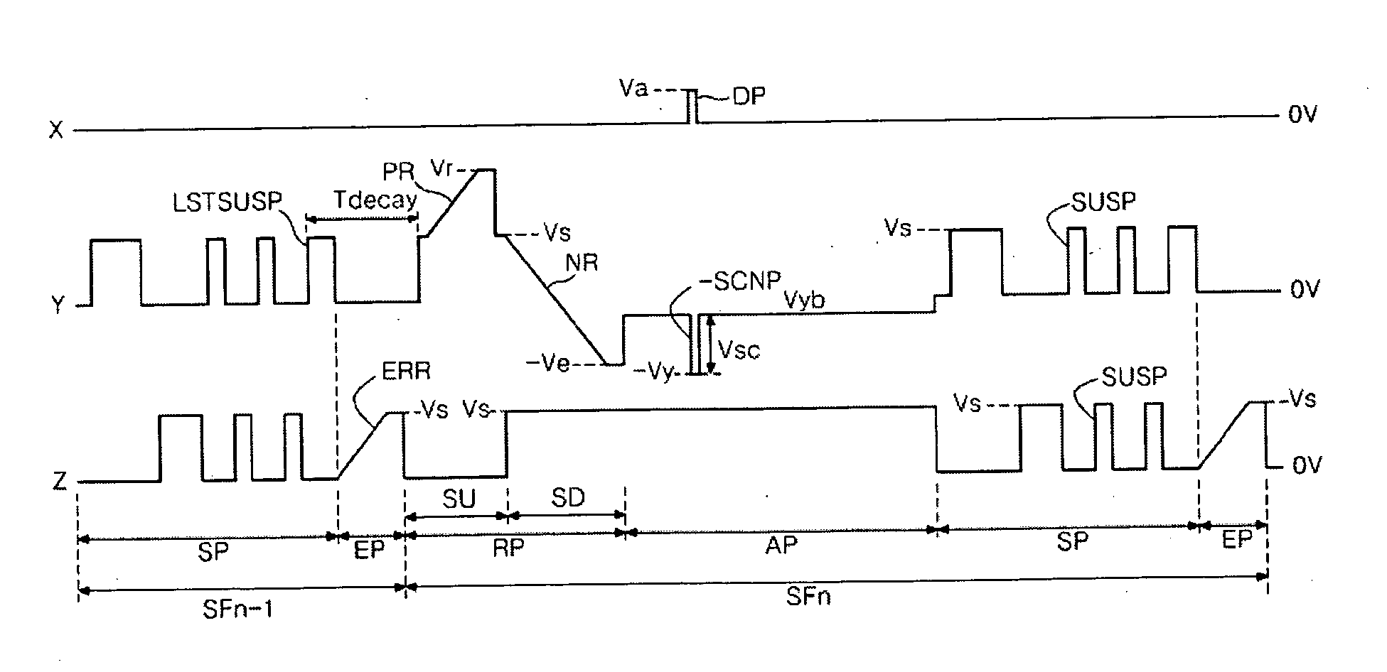
[0090]FIG. 9 is a wave form view illustrating a driving method for a plasma display apparatus according to the present invention. The driving wave form of FIG. 9 is applied to a three-electrode alternate current surface discharge type plasma display panel (PDP) similar to FIG. 2. In FIG. 9, each of sub-fields (SFn−1, SFn) includes a reset period (RP) for initializing discharge cells of a whole image, an address period (AP) for selecting the discharge cell, a sustain period (SP) for sustaining the discharge of the selected discharge cells, and an erasure period (EP) for erasing wall charges in the discharge cell 1.
[0091] The reset period (RP), the address period (AP) and the sustain period (SP) are the same as those of a driving wave form of FIG. 3 and accordingly, a detailed description thereof is omitted.
[0092] In the driving method for the plasma display apparatus according to the first embodiment of the present invention, it is assumed that the plasma display panel has a first t...
second embodiment
[0096]FIG. 10 is a wave form view illustrating a driving method for a plasma display apparatus according to the present invention.
[0097] The driving wave form of FIG. 10 is applicable to the PDP where the discharge cell can be initialized using only the last sustain discharge of a previous sub-field without a set-up discharge and its subsequent set-down discharge of a next sub-field, that is, to the PDP having a high uniformity and a wide driving margin of the discharge cells.
[0098] Referring to FIG. 10, the (n−1)th sub-field (SFn−1) includes a reset period (RP), an address period (AP), and a sustain period (SP). The nth sub-field(SFn) includes a reset period (RP) having only a set-down period without a set-up period, an address period (AP), a sustain period (SP), and an erasure period (EP).
[0099] The address period (AP) and the sustain period (SP) are the same as those of the driving wave form of FIG. 3 and the embodiment of FIG. 9 and accordingly, a detailed description thereof ...
third embodiment
[0103]FIG. 11 is a wave form view illustrating a driving method for a plasma display apparatus according to the present invention. The driving wave form of FIG. 11 is described with reference to the wall charge distribution of FIGS. 12A to 12E.
[0104] In FIG. 11, the plasma display apparatus is driven by dividing at least one sub-field, for example, a first sub-field into a pre-reset period (PRERP), a reset period (RP), an address period (AP), and a sustain period (SP). During the pre-reset period (PRERP), positive wall charges are formed on scan electrodes (Y) and negative wall charges are formed on sustain electrodes (Z). During the reset period (RP), discharge cells of a whole image are initialized using a wall charge distribution, which is formed during the pre-reset period (PRERP). During the sustain period (SP), a discharge of the selected discharge cells is sustained. An erasure period can be included between the sustain period (SP) and the reset period of its next sub-field. ...
PUM
 Abstract
Description
Claims
Application Information