Eureka AIR delivers breakthrough ideas for toughest innovation challenges, trusted by R&D personnel around the world.

Manufacturing method and luminance adjustment method of light emitting element array, exposure head, and electrophotographic apparatus

Inactive Publication Date: 2006-06-01
PANASONIC CORP
View PDF2 Cites 13 Cited by
  • Summary
  • Abstract
  • Description
  • Claims
  • Application Information

AI Technical Summary

Benefits of technology

[0010] The invention is proposed in view of the above-mentioned problems, and has objects of providing a light emitting element array and an exposure head capable of reducing the light volume dispersion by a simple configuration, and a manufacturing method and a light volume adjustment method thereof, and a suitable electrophotographic apparatus mounted the exposure head.

Problems solved by technology

Where the exposure head is provided with a number of light emitting elements like the exposure head for the high resolution, there are problems such as increasing a space to mount the correction circuit, increasing assembly process steps of the exposure head, and the like.
However, improving the manufacturing accuracy in the microfabrication is not preferable because the manufacturing cost increase instantly due to such improvement.
However, when the exposure head is formed by a plurality of elements disposed linearly and widely as mentioned above, there is a possibility that the time-dependent behavior of the light volume degradation will not be the same on each element disposed on both sides.
When each light emitting element used to the same exposure head has a different time dependency of the light volume degradation, even if the lighting count (the lighting time) is made to be identical approximately for every element, the light volume degradation cannot be corrected.

Method used


Image

  • Manufacturing method and luminance adjustment method of light emitting element array, exposure head, and electrophotographic apparatus
  • Manufacturing method and luminance adjustment method of light emitting element array, exposure head, and electrophotographic apparatus
  • Manufacturing method and luminance adjustment method of light emitting element array, exposure head, and electrophotographic apparatus

Examples


Embodiment Construction

[0051] Embodiments of the invention are discussed here in details according to attached drawings.

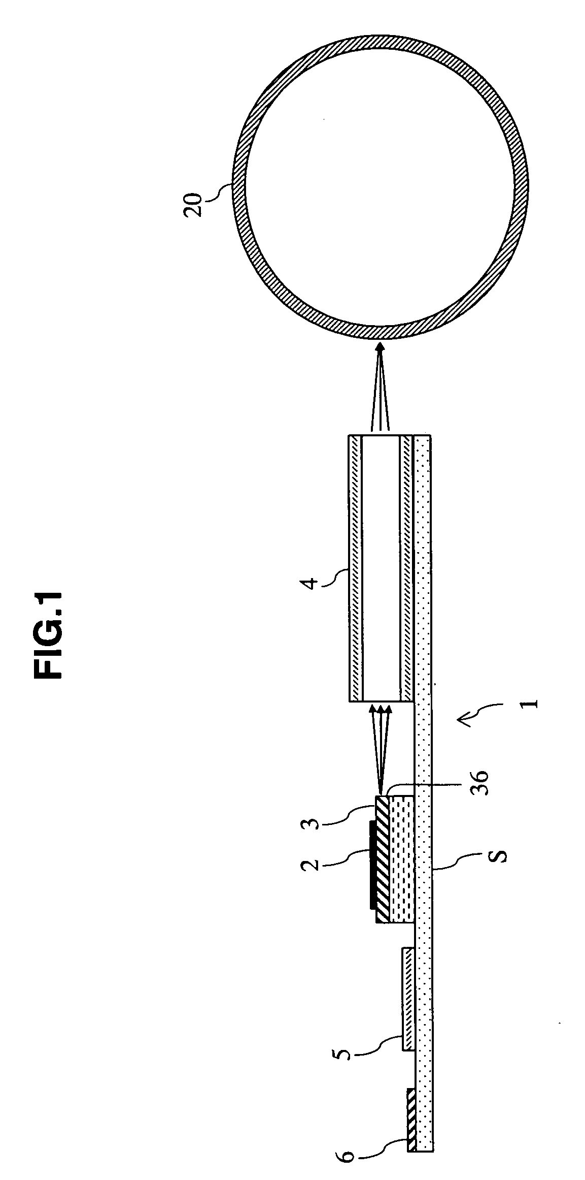
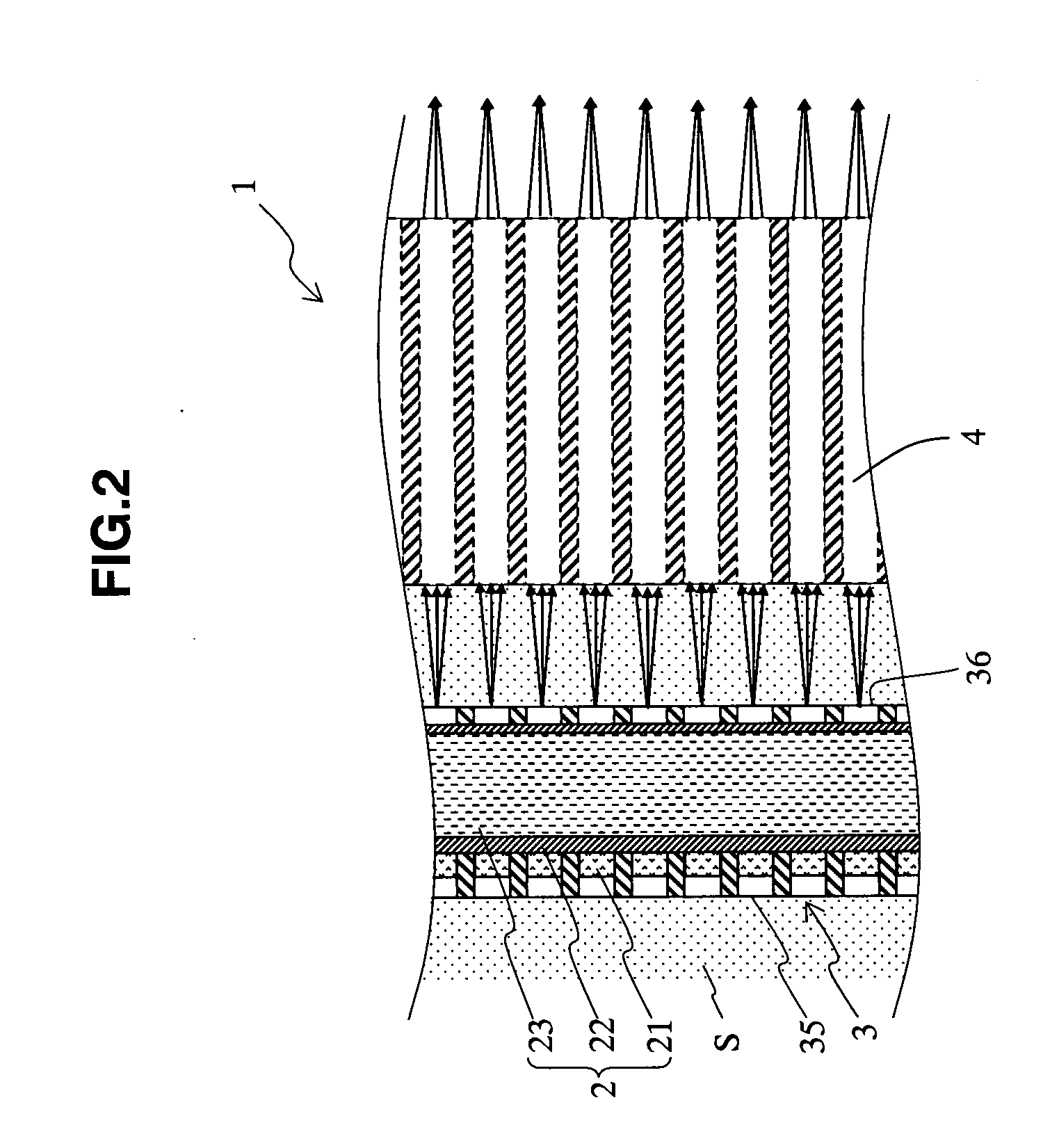
[0052] A basic structure of an exposure light of the invention is schematically illustrated according to a sectional view in FIG. 1 and a plane view of a relevant part in FIG. 2. FIG. 1 and FIG. 2 show examples of the exposure head structure suitable for the high resolution particularly, and the structure of the exposure head of the invention is not limited only to this structure.

[0053] As shown in FIG. 1, an exposure head 1 of the invention is provided with a light emitting element array 2, a light guide plate 3, and a lens array 4 on a substrate S made of glass, a metal and so. The light emitting element array 2 (which will be described as a light emitting element 2, according to need) is formed by a plurality of organic EL elements that are disposed linearly along a width direction of a photoconductor 20 on which a latent image is formed. The light guide plate 3 guides light from th...


PUM


Abstract

As for a light emitting array and an exposure head provided with a plurality of light emitting elements capable of emitting light by the supplying power respectively, the electrical stress is given only to the light emitting element selected based on the luminance of each light emitting element, whereby the luminance of the light emitting element is reduced. According to such configuration, it is possible to provide the light emitting array with the small light volume dispersion, and the exposure head, and the electrophotographic apparatus thereof.

Description

FIELD OF THE INVENTION [0001] The invention relates to a light emitting element array and an exposure head that are provided with a plurality of light emitting elements capable of emitting light by supplying power respectively, a manufacturing method of the light emitting element array and the exposure head, a luminance adjustment method of the light emitting element array, and an electrophotographic apparatus with the exposure head. BACKGROUND OF THE INVENTION [0002] An electrophotographic apparatus forms a latent image on a photoconductive drum, for example, by light emitted from an exposure head provided with a plurality of light emitting elements, and then forms an image on a paper based on the latent image. In such electrophotographic apparatus, each light volume of light emitted from the exposure head must be even so that thus formed image on the paper does not have density dispersion. [0003] However, in LED (Light Emitting Device) generally used as the light emitting element,...

Claims


Application Information

Patent Timeline
IPC IPC(8): H01L21/00
CPCG06K15/1247
Inventor MASUMOTO, KENICHI
Owner PANASONIC CORP
Why Eureka
Eureka Blog
Learn More