Liquid crystal display device and method of fabricating the same

Active Publication Date: 2006-06-08
LG DISPLAY CO LTD
View PDF14 Cites 11 Cited by
  • Summary
  • Abstract
  • Description
  • Claims
  • Application Information

AI Technical Summary

Benefits of technology

[0015] An object of the present invention is to provide an LCD device that prevents formation of bubbles during liquid crystal injection processing.
[0016] Another

Problems solved by technology

Accordingly, defects are generated in the LCD panel

Method used


Image

  • Liquid crystal display device and method of fabricating the same
  • Liquid crystal display device and method of fabricating the same
  • Liquid crystal display device and method of fabricating the same

Examples


Example

[0029] Reference will now be made in detail to the preferred embodiments of the present invention, examples of which are illustrated in the accompanying drawings.

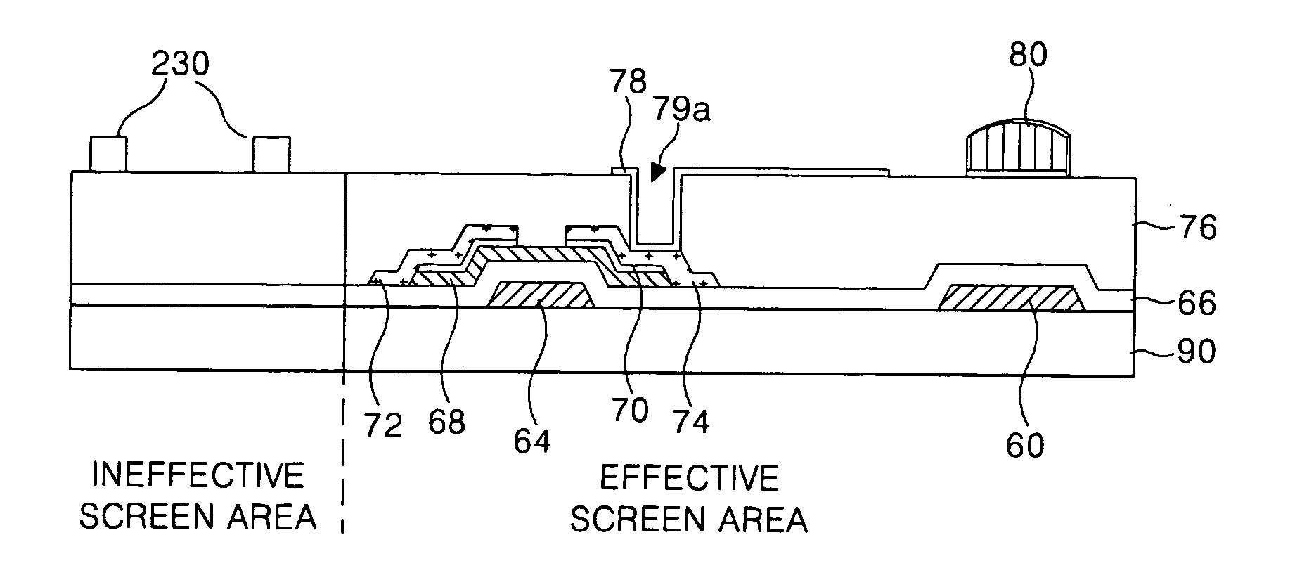
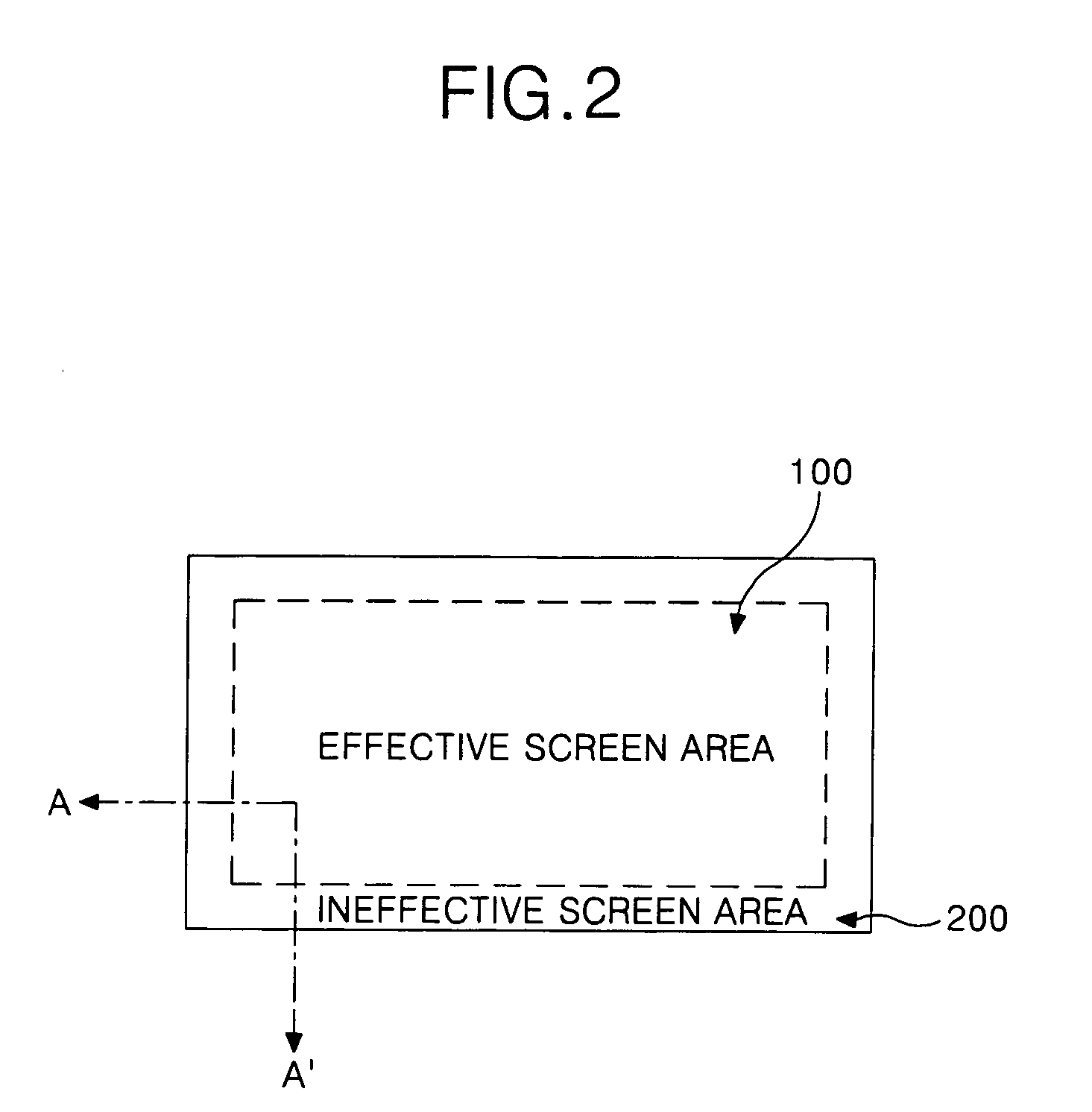
[0030]FIG. 2 is a schematic plan view of an exemplary screen display area of an LCD device according to the present invention. In FIG. 2, an LCD device may include an display screen area 100 where liquid crystal display elements are arranged to display images, and an indisplay screen area 200 at the outer part of the display screen area. In the display screen area 100, the liquid crystal display elements are arranged to display images in accordance with data signals supplied from a drive circuit (not shown). In addition, in the indisplay screen area 200, a sealant is formed for bonding the upper array substrate and the lower array substrate during a substrate bonding / liquid crystal injection process during fabrication of the LCD device.

[0031]FIG. 3 is a schematic plan view of an exemplary LCD panel according to the presen...


PUM


Abstract

A liquid crystal display device includes a liquid crystal display panel having a liquid crystal area defined within a display area by a sealant, and a non-display area formed in an outer part of the display area, and at least one bubble trap arranged in the outer part of the sealant within the non-display area and patterned to have a concave surface facing toward outside of the non-display area.

Description

[0001] The present application claims the benefit of the Korean Patent Application No. P2004-101448 filed in Korea on Dec. 3, 2004, which is hereby incorporated by reference. BACKGROUND OF THE INVENTION [0002] 1. Field of the Invention [0003] The present invention relates to a liquid crystal display (LCD) device, and more particularly to an LCD device that prevents formation of bubbles at an display screen area where an image is displayed, and to a method of fabricating an LCD device that controls formation of bubbles which is generated during a process of injecting liquid crystal. [0004] 2. Description of the Related Art [0005] In general, an LCD device controls light transmissivity of liquid crystal material by application of an electric field in order to display images. Accordingly, the LCD device includes a liquid crystal display panel having liquid crystal cells arranged in a matrix configuration and a drive circuit in order to drive the liquid crystal display panel. The liquid...

Claims


Application Information

Patent Timeline
IPC IPC(8): G02F1/1339G02F1/1333G02F1/1341
CPCG02F1/1339G02F1/1341
Inventor BAEK, SE JOONSON, HAE JOON
Owner LG DISPLAY CO LTD
Why Eureka
Try Eureka