Connection structure and fabrication method for the same

Inactive Publication Date: 2007-07-26
PANASONIC CORP
View PDF0 Cites 10 Cited by
  • Summary
  • Abstract
  • Description
  • Claims
  • Application Information

AI Technical Summary

Benefits of technology

[0016]The material TiN in the contact plug in the conventional technology serves as a reaction prevention layer for preventing solid phase reaction between the silicide film and metal during heat treatment. However, the contact plug is unable to suppress growth of a degenerated layer in a process preceding the for

Problems solved by technology

However, the contact plug is unable to suppress growth of a degener

Method used


Image

  • Connection structure and fabrication method for the same
  • Connection structure and fabrication method for the same
  • Connection structure and fabrication method for the same

Examples


Example

Embodiment 1

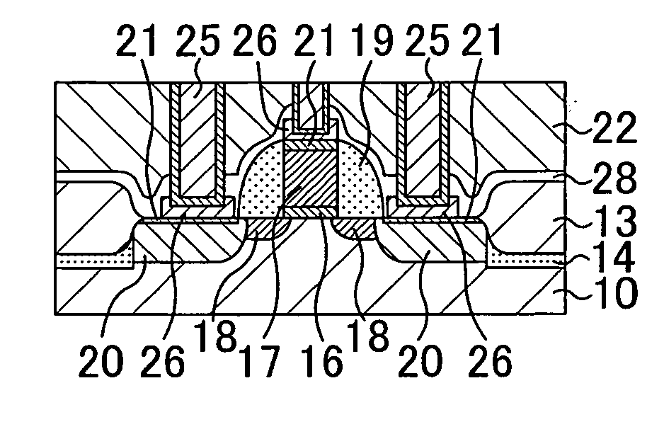
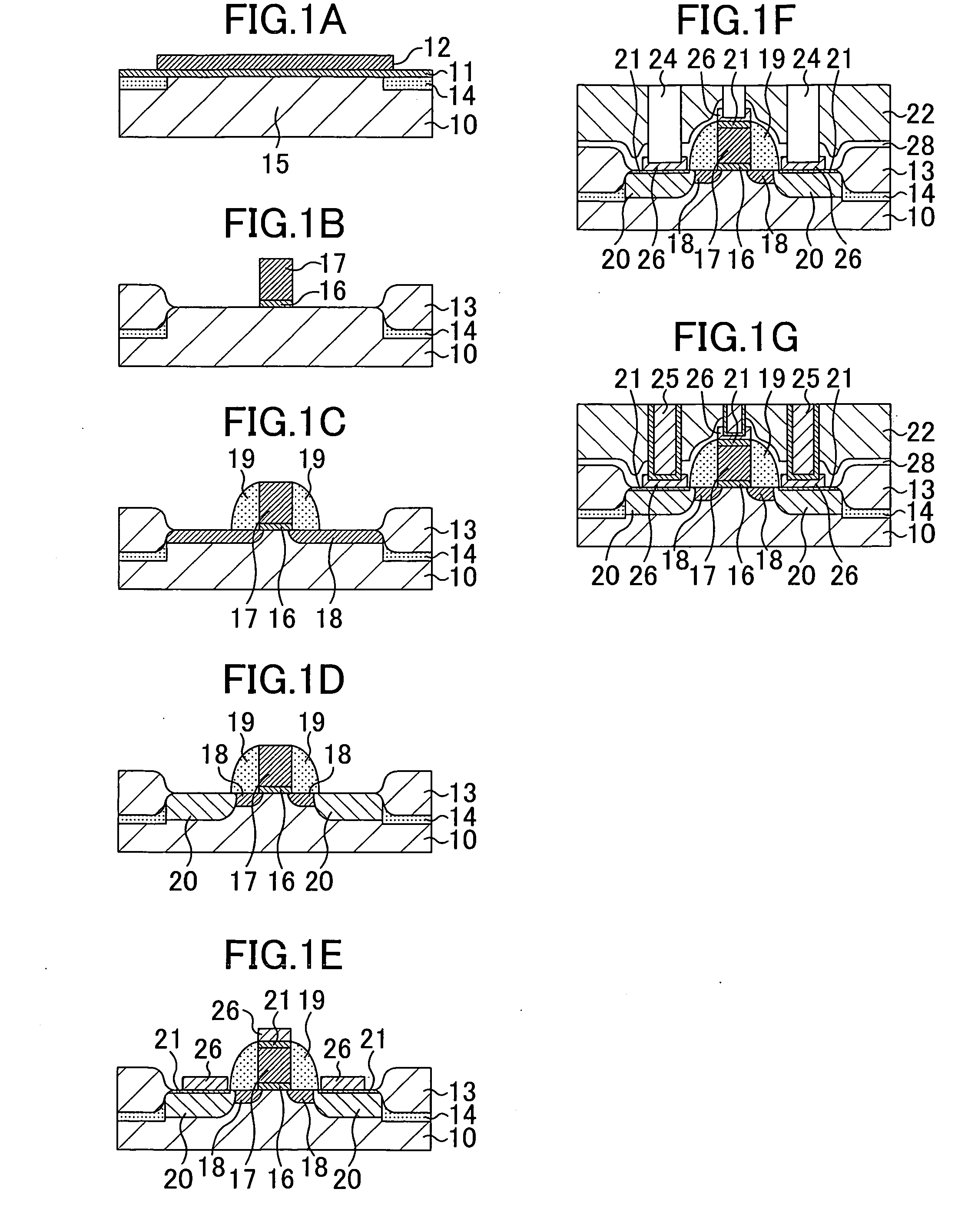
[0047]A fabrication method for a connection structure in Embodiment 1 of the present invention will be described with reference to FIGS. 1A through 1G. FIGS. 1A through 1G are cross-sectional views showing process steps of the fabrication method in Embodiment 1.

[0048]In this embodiment, description will be made focusing attention on one NMIS transistor and its surroundings constituting a semiconductor integrated circuit device.

[0049]In the fabrication method for a connection structure in this embodiment, first, as shown in FIG. 1A, a p-type impurity such as boron is ion-implanted in a predetermined region of a silicon substrate 10 doped with an n-type impurity, to form a p-well 15. A silicon oxide film 11 and a silicon nitride film 12 are then deposited on the n-type impurity-doped silicon substrate 10. A resist pattern (not shown) is formed by lithography, and using the resist pattern as a mask, the silicon nitride film 12 is then patterned by reactive ion etching. The ...

Example

Embodiment 2

[0065]A fabrication method for a connection structure in Embodiment 2 of the present invention will be described with reference to FIGS. 3A through 3E. FIGS. 3A through 3E are cross-sectional views showing process steps of the fabrication method in Embodiment 2.

[0066]In the fabrication method in this embodiment, the method in Embodiment 1 is followed until the formation of the source / drain regions 20 as shown in FIG. 3A.

[0067]Thereafter, as shown in FIG. 3B, Ni is deposited to a thickness of 15 nm by sputtering and then subjected to first heat treatment in a nitrogen atmosphere, to form silicide films 21 on the Si-exposed source / drain regions 20 and gate electrode 17. Selective etching is then performed using wet etching to remove unreacted Ni. As an example of conditions for the wet etching, a liquid mixture of sulfuric acid and hydrogen peroxide, for example, may be used. Thereafter, the silicide films 21 are subjected to second heat treatment to reduce the resistance ...

Example

Embodiment 3

[0076]A fabrication method for a connection structure in Embodiment 3 of the present invention will be described with reference to FIGS. 4A through 4E. FIGS. 4A through 4E are cross-sectional views showing process steps of the fabrication method in this embodiment.

[0077]In the fabrication method in this embodiment, the method in Embodiment 1 is followed until the formation of the source / drain regions 20 as shown in FIG. 4A.

[0078]Thereafter, as shown in FIG. 4B, Ni is deposited to a thickness of 15 nm by sputtering, and then subjected to first heat treatment in a nitrogen atmosphere to form silicide films 21 on the Si-exposed source / drain regions 20 and gate electrode 17. Selective etching is then performed using wet etching to remove unreacted Ni. As an example of condition for the wet etching, a liquid mixture of sulfuric acid and hydrogen peroxide, for example, may be used. Thereafter, the silicide films 21 are subjected to second heat treatment to reduce the resistanc...


PUM


Abstract

A conductive layer is formed in or on a substrate. A first metal film is then formed on the substrate including the conductive layer. The substrate is then subjected to heat treatment to allow the first metal film to react with the conductive layer to thereby form a silicide film selectively on the conductive layer. A second metal film is then formed only on the silicide film by selective CVD. An insulating film is then formed over the substrate including the second metal film. A predetermined region of the insulating film is removed to form a contact hole reaching the second metal film. The inside of the contact hole is cleaned to remove a degenerated layer formed on the surface of the second metal film existing on the bottom of the contact hole.

Description

CROSS-REFERENCE TO RELATED APPLICATIONS[0001]The disclosure of Japanese Patent Application No. 2006-016073 filed Jan. 25, 2006 including specification, drawing and claims is incorporated herein by reference in its entirely.BACKGROUND OF THE INVENTION[0002]The present invention relates to a connection structure and a fabrication method for the same, and more particularly, to a structure of a connection portion in a semiconductor device and a fabrication method for the same.[0003]In semiconductor integrated circuit devices, as semiconductor elements have been made finer with the trend of higher speed and higher integration, it has become essential to form shallow diffusion layers as source / drain regions. By making diffusion layers shallow, however, the resistance of the diffusion layers becomes high, and a problem arises that the contact resistance between the diffusion layers and plugs forming connections with the diffusion layers becomes extremely high.[0004]Conventionally, as a gen...

Claims


Application Information

Patent Timeline
IPC IPC(8): H01L29/40H01L21/44
CPCH01L21/28518H01L21/76814H01L21/76829H01L29/66515H01L21/76885H01L29/665H01L21/76843H01L23/485
Inventor GOTO, SATORU
Owner PANASONIC CORP
Why Eureka
Try Eureka