Method for forming self-aligned dual salicide in CMOS technologies

a technology of self-aligning and dual salicide, which is applied in the direction of semiconductor/solid-state device manufacturing, basic electric elements, electric apparatus, etc., can solve the problems of inferior device/circuit performance, non-optimal device performance, and misalignment caused, so as to simplify the dual salicide formation process and reduce the required lithography level , the effect of eliminating the problem of misalignmen

Inactive Publication Date: 2006-06-08
AURIGA INNOVATIONS INC
View PDF9 Cites 4 Cited by
  • Summary
  • Abstract
  • Description
  • Claims
  • Application Information

AI Technical Summary

Benefits of technology

[0017] Generally, the embodiments of the invention provide a double self-aligning technique of forming a dual salicide (i.e., different salicide formations), such as NiSi, CoSi2, TiSi2, WSi2, PdSi, PtSi, TaSi2, ReSi, etc., and their alloys at the source/drain and gate areas for NFET and PFET regions of a CMOS device with only one lithography level. As such, the embodiments of th

Problems solved by technology

However, one of the drawbacks of this approach is non-optimal device performance when compared with a dual salicide approach.
However, one of the problems with the conventional two lithography level dual salicide process as provided in FIGS. 2-4 is the misalignment caused during the processing between the two lithography levels as illustrated in FIG. 5 (the dotted circle represents the

Method used


Image

  • Method for forming self-aligned dual salicide in CMOS technologies
  • Method for forming self-aligned dual salicide in CMOS technologies
  • Method for forming self-aligned dual salicide in CMOS technologies

Examples


first embodiment

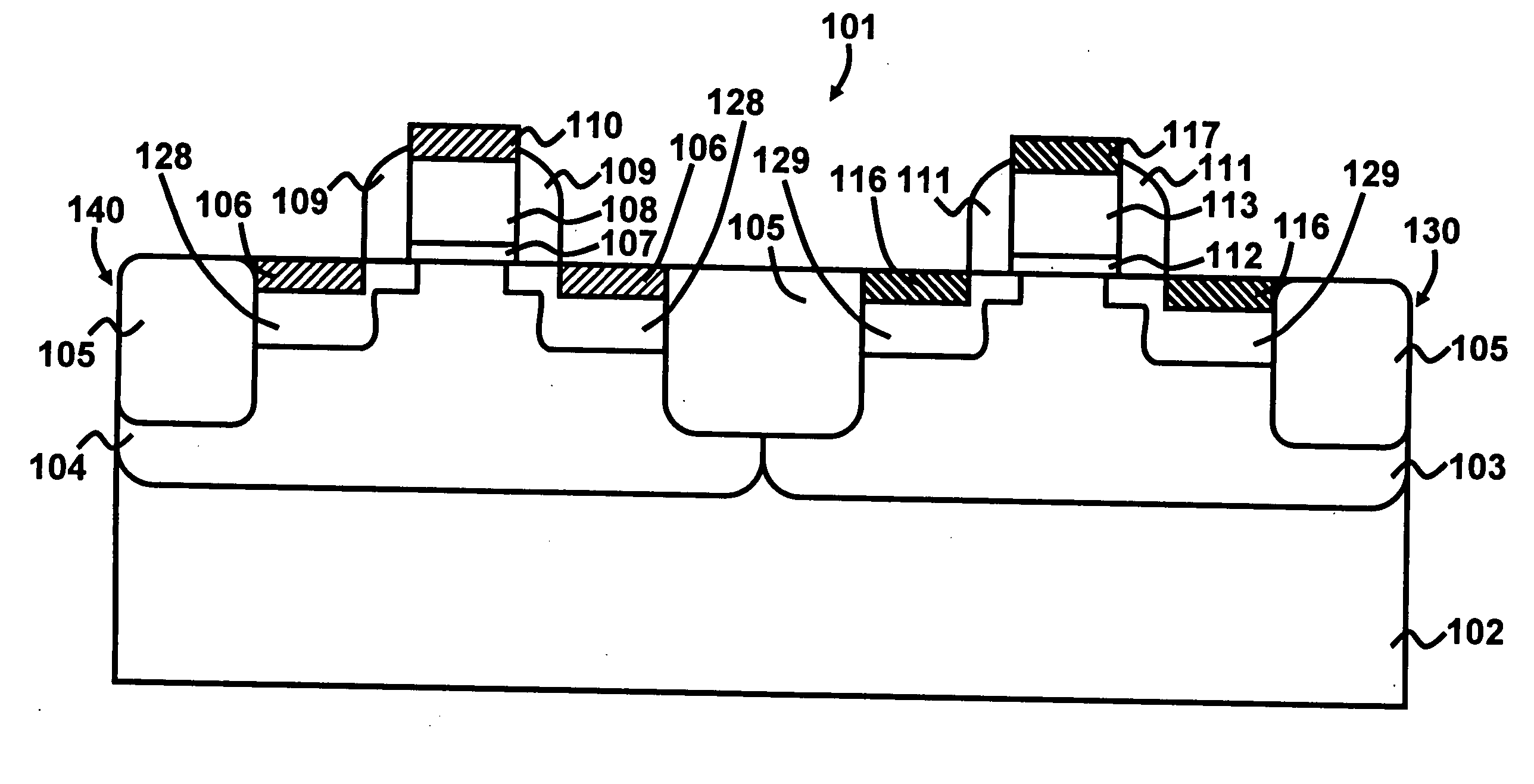
[0034] Next, as illustrated in FIG. 8, the silicide blocking film 114 is removed from the device 101, and a second metal layer123 is deposited over the entire device 101 (i.e., over both the NFET 140 and PFET 130 regions). Optionally, a cap layer (not shown) may be formed over the second metal layer 123 to prevent oxidation of the silicide during the subsequent annealing process. Furthermore, those skilled in the art would readily understand how to incorporate the optional capping layer over the second metal layer 123. Thereafter, as depicted in FIG. 9, after an annealing process is conducted, the resulting silicide layer 117 over the PFET gate 113 as well as the source / drain silicide contacts 116 on opposite sides of the PFET gate 113 is formed. As shown in FIG. 9, the silicide on the NFET portion 140 of the device 101 is different from the silicide on the PFET portion 130 of the device 101. Moreover, the dual salicide process provided by the invention is performed with only one li...

second embodiment

[0045]FIG. 18 illustrates the process flow according to the invention, which describes a method of forming metal silicide layers over a semiconductor substrate 202, wherein the method comprises forming (501) a first well region 203 in the semiconductor substrate 202 for accommodating a first type semiconductor device 230; forming (503) a second well region 204 in the semiconductor substrate 202 for accommodating a second type semiconductor device 240; selectively forming (505) a first metal layer 221 over the second type semiconductor device 240; depositing (507) a capping layer 222 over the first metal layer 221; depositing (509) a second metal layer 223 over the capping layer 222 and the first type semiconductor device 230; and performing (511) a salicide formation on the first and second type semiconductor devices 230, 240, wherein the process of performing (511) the salicide formation is accomplished by annealing the first and second metal layers 221, 223, removing the capping l...


PUM


Abstract

A method of fabricating a complementary metal oxide semiconductor (CMOS) device, wherein the method comprises forming a first well region in a semiconductor substrate for accommodation of a first type semiconductor device; forming a second well region in the semiconductor substrate for accommodation of a second type semiconductor device; shielding the first type semiconductor device with a mask; depositing a first metal layer over the second type semiconductor device; performing a first salicide formation on the second type semiconductor device; removing the mask; depositing a second metal layer over the first and second type semiconductor devices; and performing a second salicide formation on the first type semiconductor device. The method requires only one pattern level and it eliminates pattern overlay as it also simplifies the processes to form different silicide material over different devices.

Description

CROSS REFERENCE TO RELATED APPLICATION [0001] This application relates to co-pending U.S. patent application Ser. No. ______ entitled “Method for Forming Self-Aligned Dual Fully Silicide Gates in CMOS Devices” (Docket No. FIS920040183US1), filed concurrently herewith, the contents of which in its entirety is herein incorporated by reference.BACKGROUND OF THE INVENTION [0002] 1. Field of the Invention [0003] The embodiments of the invention generally relate to complementary metal oxide semiconductor (CMOS) device fabrication, and more particularly to a method of forming dual self-aligned silicide in CMOS technologies to improve device performance. [0004] 2. Description of the Related Art [0005] The term salicide, which stands for Self-ALIgned siliCIDE, refers to a silicide formed by a self-aligning method. A salicide is typically formed by depositing a metal layer (such as Ti, Co, Ni, etc.) over a silicon layer, and then annealing the semiconductor structure. Where the metal is in co...

Claims


Application Information

Patent Timeline
IPC IPC(8): H01L21/8238H01L21/3205H01L21/44
CPCH01L21/28518H01L21/823814H01L21/823835H01L21/8238
Inventor FANG, SUNFEICABRAL, CYRIL JR.DZIOBKOWSKI, CHESTER T.ELLIS-MONAGHAN, JOHN J.LAVOIE, CHRISTIANLUO, ZHIJIONGNAKOS, JAMES S.STEEGEN, AN L.WANN, CLEMENT H.
Owner AURIGA INNOVATIONS INC
Why Eureka
Try Eureka