Resistive structure integrated in a semiconductor substrate

Inactive Publication Date: 2006-06-15
STMICROELECTRONICS SRL
View PDF3 Cites 0 Cited by
  • Summary
  • Abstract
  • Description
  • Claims
  • Application Information

AI Technical Summary

Benefits of technology

[0036] The principle on which this invention stands is one of providing a resistive structure which is isolated dielectrically, integrated in a semiconductor substrate, suitable for low- and high-voltage applications, and occupies far less silicon area t

Problems solved by technology

On the one hand, integrating high-voltage resistive structures of conventional design requires fairly large silicon space, i.e., chip surface space, even when resistive layers with the highest resistance allowed by technology are provided.
However, this layout also is difficult to use with high-voltage resistive structures, on account of its heavy silicon space requirements.
Consequently, the spread of this depletion region would

Method used


Image

  • Resistive structure integrated in a semiconductor substrate
  • Resistive structure integrated in a semiconductor substrate
  • Resistive structure integrated in a semiconductor substrate

Examples


third embodiment

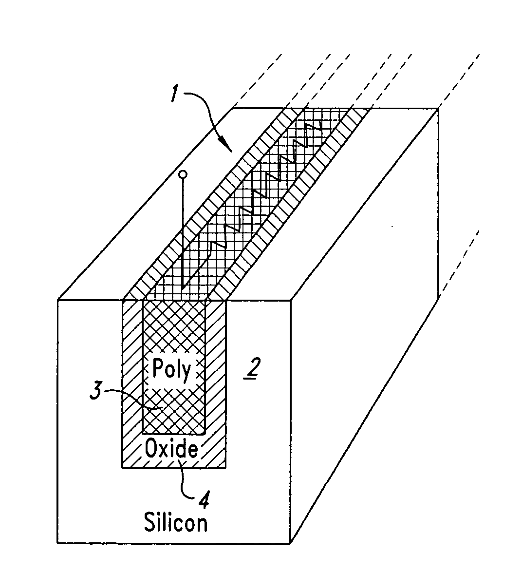
[0065] a dielectrically isolated resistive structure according to the invention is shown generally and schematically at 91 in FIG. 9.

[0066] In particular, the rungs of the resistive structure 91 are connected together in parallel by a metallization 95. The equivalent resistance of the resulting structure is, therefore, n times smaller than the resistance of each rung of the structure, n being the number of rungs linked together by the metallization 95.

[0067] In this way, resistive structures of controlled resistance can be obtained by the resistance of each rung of the resistive structure according to the invention can be set in a positive manner, these being resistive elements formed from polysilicon and isolated dielectrically.

fourth embodiment

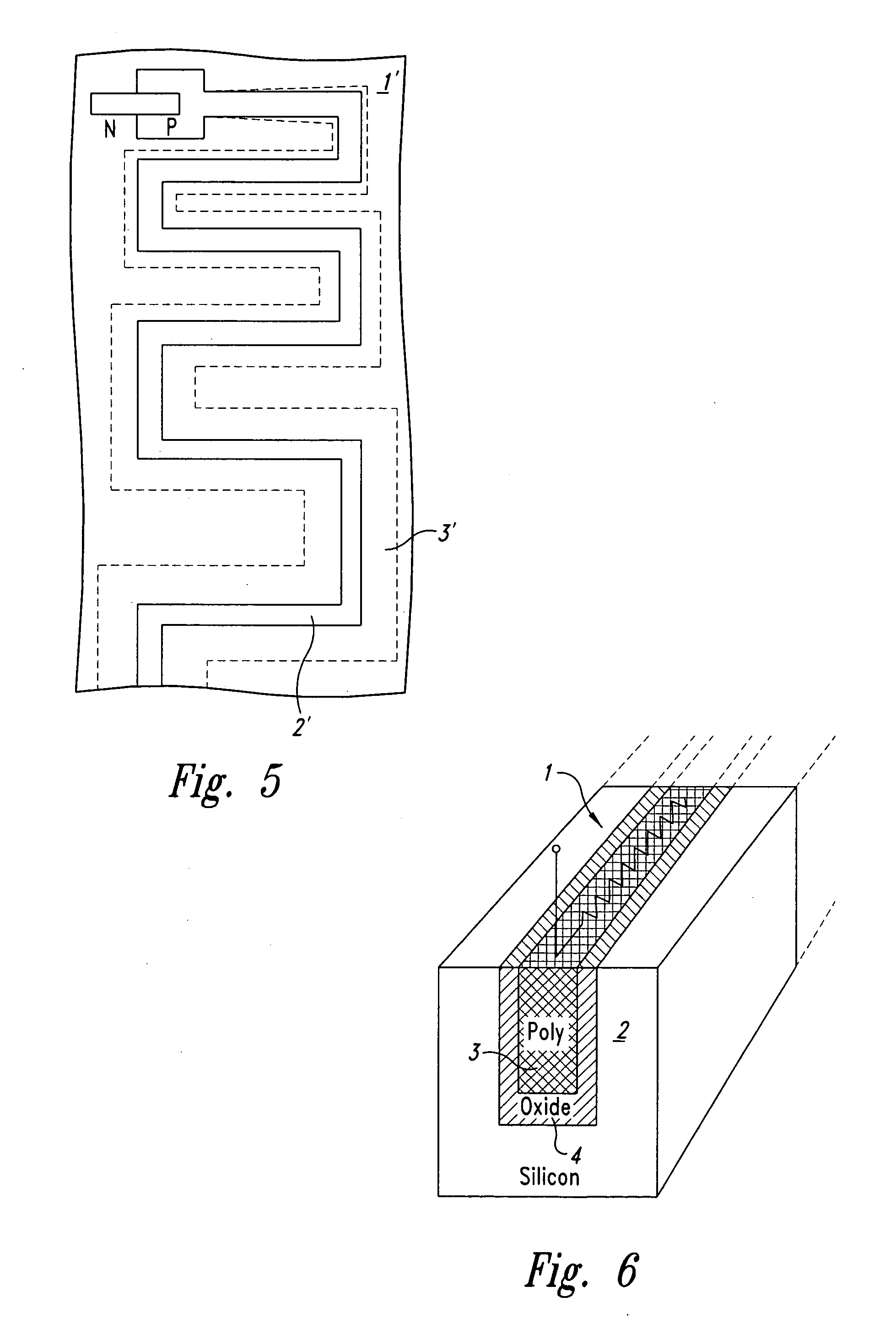
[0068] Shown in FIG. 10 is the resistive structure according to the invention, generally designated 101.

[0069] In particular, the resistive structure 101 is formed in a semiconductor substrate 102 using a polysilicon fill layer 103 of an oxide trench 104, the layer 103 being masked off and then etched away to yield a T-shaped structure 106, as shown in FIG. 10, rather than being planarized by a chemical etching step across its surface.

[0070] In other words, the T-shaped structure 106 retains polysilicon connection paths. Low-resistance resistive structures are thus provided which can be connected to other components through this T-shaped structure 106, being integral with the resistive structure and functioning as field plates in the instance of high-voltage applications.

[0071] Advantageously in this invention, all of the above-discussed embodiments of the dielectrically isolated resistive structure utilize a fill polysilicon of the dielectric trenches which is suitably doped eith...


PUM


Abstract

A resistive structure integrated in a semiconductor substrate and having a suitably doped polysilicon region that is completely surrounded by a dielectric region so that the resistive structure is isolated electrically from other components jointly integrated in the semiconductor substrate.

Description

BACKGROUND OF THE INVENTION [0001] 1. Field of the Invention [0002] This invention relates to a resistive structure integrated in a semiconductor substrate, and more specifically to a resistive structure integrated in a semiconductor substrate and having a suitably doped polysilicon region. [0003] The invention relates, particularly but not exclusively, to a high-voltage resistive structure for integration in a semiconductor substrate along with power devices, and this description covers this field of application for convenience of illustration only. [0004] 2. Description of the Related Art [0005] As is well known, high-voltage resistive structures integrated in a semiconductor substrate are used extensively in IC power devices, e.g., VIPower devices. [0006] VIPower devices have a region where power devices are formed (power region) and a region where signal devices are formed (signal region) jointly integrated in the same chip. Some applications require that provisions be made in t...

Claims


Application Information

Patent Timeline
IPC IPC(8): H01L29/00H01L21/02H01L27/08
CPCH01L27/0802H01L28/20
Inventor LEONARDI, SALVATOREMODICA, ROBERTO
Owner STMICROELECTRONICS SRL
Why Eureka
Try Eureka