

Method and apparatus for manufacturing active-matrix organic el display, active matrix organic el display, method for manufacturing liquid crystal array, liquid crystal array, method and apparatus for manufacturing color filter substrate, and color filter substrate
- Summary
- Abstract
- Description
- Claims
- Application Information
AI Technical Summary
Benefits of technology
Problems solved by technology
Method used
Image

Examples
embodiment 1
[0193] The following describes a preferred embodiment of the present invention with reference to the drawings. First described, with reference to FIG. 1, is an electrostatic attraction type inkjet apparatus for use in manufacturing an active matrix type organic EL display element of the present embodiment.
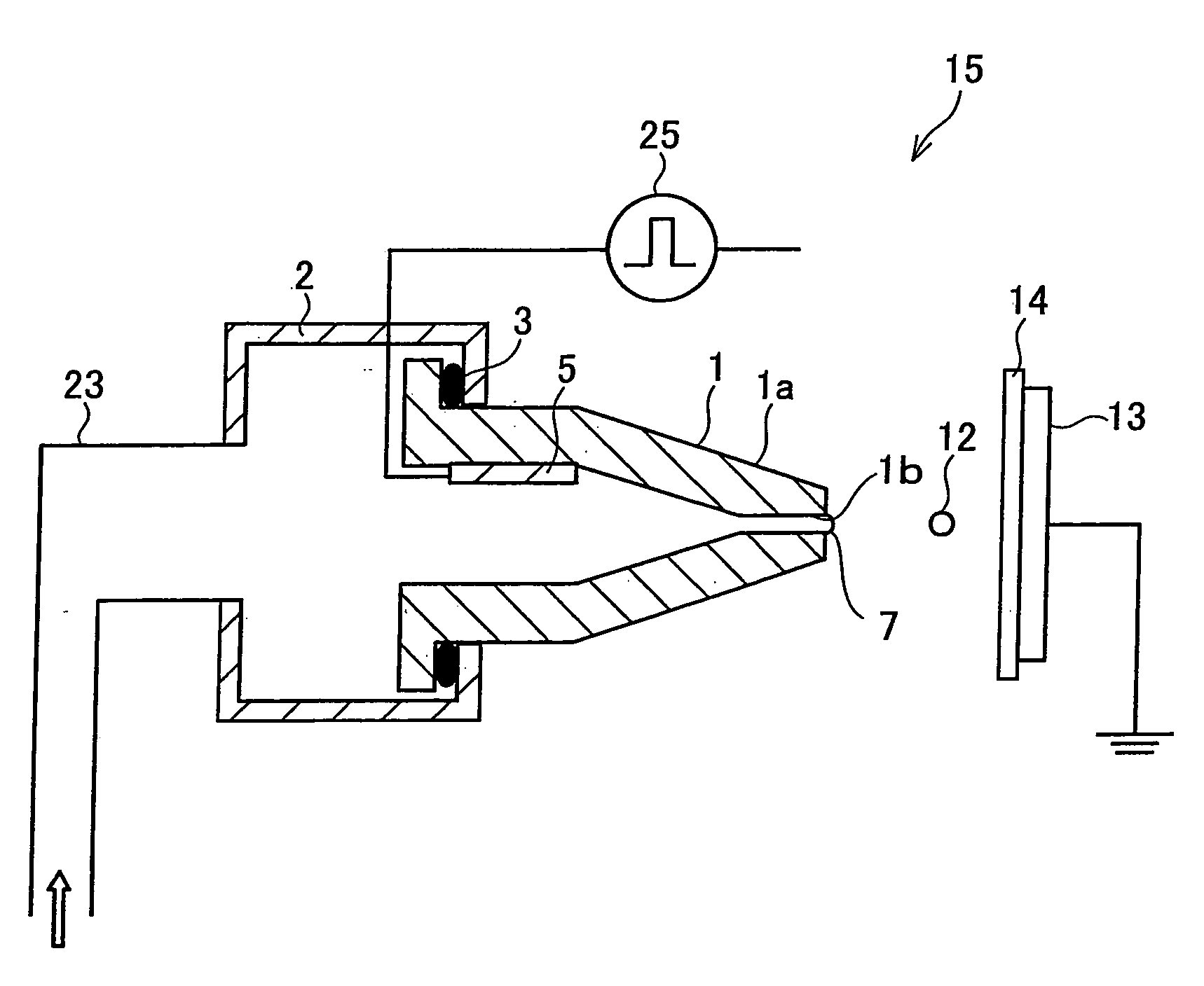
[0194]FIG. 1 is a longitudinal sectional view of an inkjet apparatus 15. The inkjet apparatus 15 is provided with a nozzle 1 for ejecting ink being stored in an ink chamber 2.
[0195] The nozzle 1 is connected with the ink chamber 2 via a packing 3. In this way, sealing is provided so that the ink in the ink chamber 2 does not leak from a joint section of the ink chamber 2 and the nozzle 1. Further, the nozzle 1 has an orifice 1a having such a shape that a diameter of the orifice 1a gradually becomes smaller toward a side opposite to the joint section of the nozzle 1 and the ink chamber 2, i. e., toward a leading edge of the nozzle 1 from which the ink is ejected. A diameter (Herei...
embodiment 3
[0387] The following explains another embodiment of the present invention.
[0388] As illustrated in FIG. 27, the liquid crystal array of the present embodiment includes spacers 181 each in the form of a column, instead of the spacers 153 having a lamination structure. Each of the spacers 181 is formed by releasing, from the nozzle 1, a material continuously in a string-like form, the material being for forming spacers. The other arrangements of the liquid crystal array of the present embodiment are the same as those of the above-described liquid crystal array. That is, the processes of forming the TFT substrate 151, the color filter substrate 152, and the alignment films 160 and 63 of the present embodiment are similar to those of Embodiment 1.
[0389] The inkjet apparatus 15 used for forming the spacers 181 is substantially the same as that used in Embodiment 1. In the arrangement of the inkjet apparatus 15 illustrated in FIG. 1, the nozzle 1 has a nozzle diameter 2 μm, and an actua...
embodiment 4
[0393] The following explains yet another embodiment of the present invention.
[0394] As illustrated in FIG. 29, the liquid crystal array of the present embodiment includes spacers 182 each in the form of a globe, instead of the spacers 153 having a lamination structure. Each of the spacers 182 is formed by ejecting, from the nozzle 1, a globular particle which becomes the spacer 182. The other arrangements of the liquid crystal array of the present embodiment are similar to those of the above-described liquid crystal array. That is, the processes of forming the TFT substrate 151, the color filter substrate 152, and the alignment films 160 and 63 of the present embodiment are similar to those of Embodiment 1.
[0395] The inkjet apparatus 15 used for forming the spacers 182 is substantially similar to that used in Embodiment 1. Note that, in the arrangement of the inkjet apparatus 15 illustrated in FIG. 1, the nozzle 1 has a nozzle diameter 8 μm, and the amount of one drop ejected fro...
PUM
 Abstract
Description
Claims
Application Information