Charge pump circuit
a charge pump and circuit technology, applied in the field of integrated circuits, can solve the problems of affecting the efficiency of the charge pump, and a large body effect of the conventional circuit, so as to reduce the influence of the body effect, improve the efficiency of the charge pump, and increase the pre-charge efficiency
- Summary
- Abstract
- Description
- Claims
- Application Information
AI Technical Summary
Benefits of technology
Problems solved by technology
Method used
Image
Examples
Embodiment Construction
[0014] The present invention relates to charge pump circuits used in integrated circuits, such as FLASH / EEPROM memory circuits. For example, the charge pump can be a PMOS negative pump circuit used to generate a relatively high negative voltage that can be applied to memory cell control gates to erase memory cell data. In one embodiment, a circuit reduces the body effect influence, which is typically present in a PMOS negative pump circuit, by using a sub-pump to increase pre-charge efficiency. In particular, the gate of the pre-charge MOSFET is pumped down to relatively very negative level. The charge pump efficiency is thereby improved.
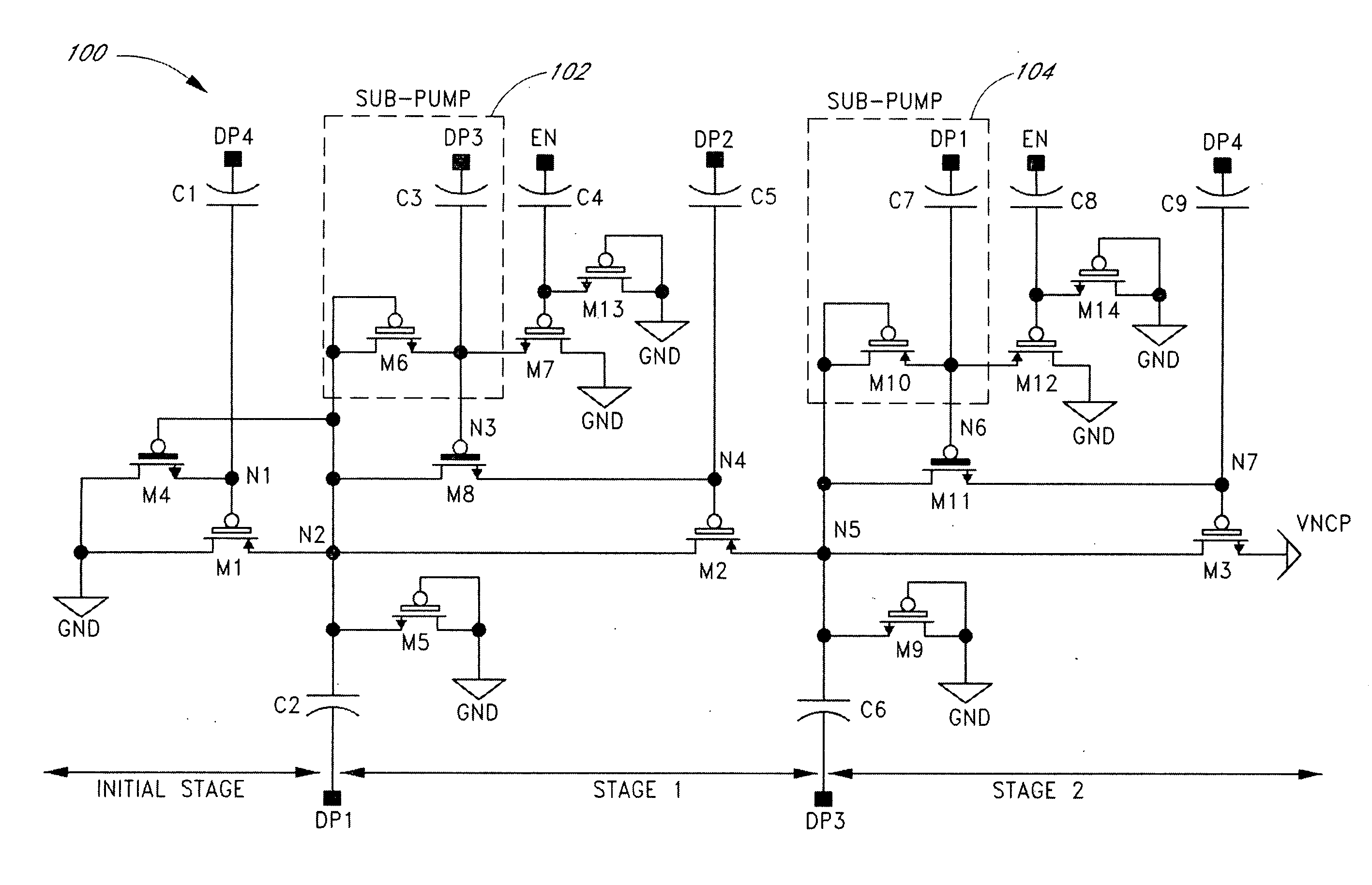
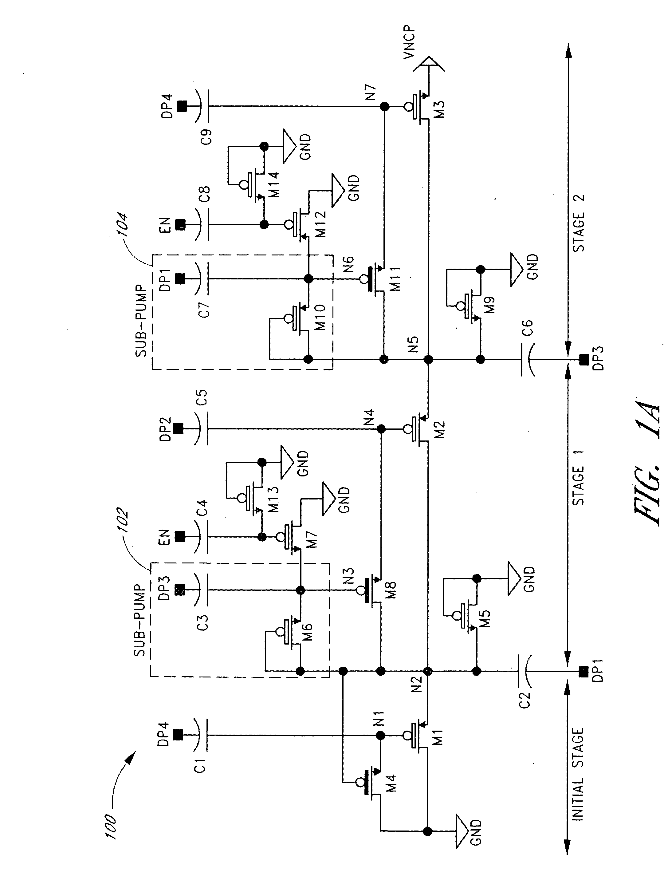
[0015]FIG. 1A illustrates an example embodiment of a P channel charge pump circuit 100. In this example, the illustrated transistors are MOSFETs. The example circuit 100 includes three stages, although other embodiments can include fewer or more stages, such as five, seven, nine, or still additional stages. For example, more stages can be connected...
PUM
 Abstract
Description
Claims
Application Information


