Image sensor test patterns for evaluating light-accumulating characteristics of image sensors and methods of testing same

a technology of image sensor and light-accumulating characteristics, which is applied in the direction of electrical equipment, semiconductor devices, radio frequency controlled devices, etc., can solve the problems of requiring a number of mask steps, high power consumption, and a relatively complex driving scheme, and achieve the effect of reducing the time required for testing

Inactive Publication Date: 2006-06-29
SAMSUNG ELECTRONICS CO LTD
View PDF7 Cites 17 Cited by
  • Summary
  • Abstract
  • Description
  • Claims
  • Application Information

AI Technical Summary

Benefits of technology

[0005] The present invention provides a test pattern of optical characteristics of a CMOS image sensor capable of reducing the time required for testing the CMOS image sensor.
[0006] The present invention also provides a test method of optical characteristics of a CMOS image sensor-capable of reducing the time required for testing the CMOS image sensor.

Problems solved by technology

The CCD has the disadvantages of a relatively complex driving scheme, high power consumption, and a complex manufacturing process requiring a number of mask steps.
Further, since the CCD cannot have a built-in signal processing circuit, it is difficult to realize the signal processing circuit in one chip.
However, this process is time consuming, which increases the production cost.

Method used


Image

  • Image sensor test patterns for evaluating light-accumulating characteristics of image sensors and methods of testing same
  • Image sensor test patterns for evaluating light-accumulating characteristics of image sensors and methods of testing same
  • Image sensor test patterns for evaluating light-accumulating characteristics of image sensors and methods of testing same

Examples


first embodiment

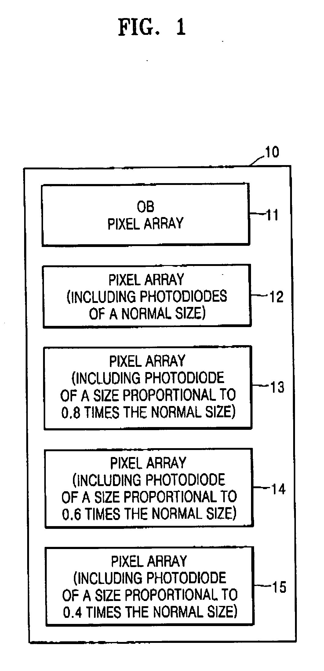
[0023] A test method of the optical characteristics of the CMOS image sensor using the test pattern will be described in detail. Generally, in the CMOS image sensor, the number of electrons which are photoelectrically converted from photons of incident light is in proportion to the size of the photodiode (PD). Specifically, the number of electrons generated at a specific luminous intensity varies depending on the size of the photodiode (PD).

[0024] In the test method using the test pattern of the optical characteristics according to the first embodiment, a test pattern region 10 for monitoring the optical characteristics is set in the CMOS image sensor chip, a pixel array 12 including photodiodes of a normal size, and a plurality of pixel array regions 13 to 15 including photodiodes of a size proportional to the normal size are located in the test pattern region 10, and then the optical characteristics of the CMOS image sensor at a single luminous intensity are tested by using the p...

second embodiment

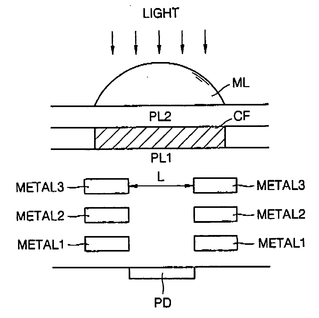
[0028] A test method of the optical characteristics of the CMOS image sensor using the test pattern will be described in detail. In the CMOS image sensor, the number of electrons which are photoelectrically converted from photons of incident light is in proportion to the size of the photodiode (PD) and the size of the open hole (L) of the photodiode (PD). Specifically, the number of electrons generated at a specific luminous intensity varies depending on the size of the open hole (L) of the photodiode (PD).

[0029] In the test method using the test pattern of the optical characteristics according to the second embodiment, a test pattern region 40 for monitoring the optical characteristics is set in the CMOS image sensor chip, a pixel array 42 including photodiodes having an open hole of a normal size and a plurality of pixel array regions 43 to 45 including photodiodes having open holes of a size proportional to the normal size are located in the test pattern region 40, and then the ...

third embodiment

[0033] A test method of the optical characteristics of the CMOS image sensor by using the test pattern will be described in detail. In the CMOS image sensor, the number of electrons which are photoelectrically converted from photons of incident light may be controlled according to the thickness and density of the color filter (CF). Specifically, the number of electrons generated at a specific luminous intensity varies depending on the thickness and density of the color filter (CF).

[0034] In the test method using the test pattern of the optical characteristics according to the third embodiment, a test pattern region 60 for monitoring the optical characteristics is set in the CMOS image sensor chip, a pixel array 62 including photodiodes having a color filter (CF) of a normal thickness and density and a plurality of pixel array regions 63 to 65 including photodiodes having color filters (CF) of a thickness or density proportional to the normal thickness or the normal density are loca...


PUM


Abstract

An image sensor test pattern provides time efficient optical testing of CMOS image senors at a single luminous intensity. These test patterns include at least first and second arrays of pixels having different light-accumulating characteristics. The different light-accumulating characteristics may be achieved multiple different ways. In some cases, the photodiodes in the first array of pixels are larger than photodiodes in the second array of pixels. In other cases, the photodiodes in the first array of pixels have open holes of a first size and the photodiodes in the second array of pixels have open holes of a second size less than the first size. In still other cases, the photodiodes in the first array of pixels have colors filters of a first density (or first thickness) and the photodiodes in the second array of pixels have color filters of a second density (or second thickness) less than the first density (or first thickness).

Description

REFERENCE TO PRIORITY APPLICATION [0001] This application claims priority to Korean Patent Application No. 2004-115046, filed Dec. 29, 2004, the disclosure of which is hereby incorporated herein by reference. FIELD OF THE INVENTION [0002] The present invention relates to image sensors and methods of testing image sensors. BACKGROUND OF THE INVENTION [0003] An image sensor is a semiconductor device for converting optical images into electric signals. Charge coupled devices (CCDs) and CMOS image sensors are examples of image sensors. The CCD is a device in which MOS capacitors are located adjacent to each other, and charge carriers are stored on each capacitor. The CMOS image sensor is a switch type device which uses a control circuit and a signal processing circuit as a peripheral circuit, with as many MOS transistors as the number of pixels, and sequentially detects outputs from the capacitors using the MOS transistors. The CCD has the disadvantages of a relatively complex driving s...

Claims


Application Information

Patent Timeline
Patent Type & Authority Applications(United States)
IPC IPC(8): H01L31/113
CPCH01L27/14603H01L27/14621H01L27/14627H01L27/14645H01L27/14685H01L27/14689H01L27/146H01L31/10
Inventor KIM, YOUNG-CHAN
Owner SAMSUNG ELECTRONICS CO LTD
Why Eureka
Try Eureka