Microelectronic packages using a ceramic substrate having a window and a conductive surface region

a technology of ceramic substrate and conductive surface, applied in the direction of electrical equipment, semiconductor devices, semiconductor/solid-state device details, etc., can solve the problems of thermal expansion mismatch, relatively high price of tapes, flip-chip configuration, etc., and achieve the effect of small cross-sectional area

Inactive Publication Date: 2006-06-29
TESSERA INC
View PDF22 Cites 54 Cited by
  • Summary
  • Abstract
  • Description
  • Claims
  • Application Information

AI Technical Summary

Problems solved by technology

However, such tapes are relatively expensive, particularly as compared to lead frames and laminate substrates.
The flip-chip configuration, however, encounters problems in thermal expansion mismatch.
When the coefficient of thermal expansion (CTE) for the device differs significantly from the CTE for the substrate, the solder connections will undergo fatigue when the package is thermally cycled.
This is particularly problematic for flip-chip packages with fine pitch, small bumps, and / or large device footprints.
However, problems associated with CTE mismatch between the wafer and the substrate are exacerbated due to the size of the wafer-scale structure.
Thus, wafer-scale manufacturing of microelectronic packages may require exceptionally close matching of device and substrate CTE.
For semiconductor-based optical devices, both ceramic and semiconductor materials have been proposed for use as substrate materials, though semiconductor materials are, as a rule, significantly more expensive than ceramic materials.

Method used


Image

  • Microelectronic packages using a ceramic substrate having a window and a conductive surface region
  • Microelectronic packages using a ceramic substrate having a window and a conductive surface region
  • Microelectronic packages using a ceramic substrate having a window and a conductive surface region

Examples


Embodiment Construction

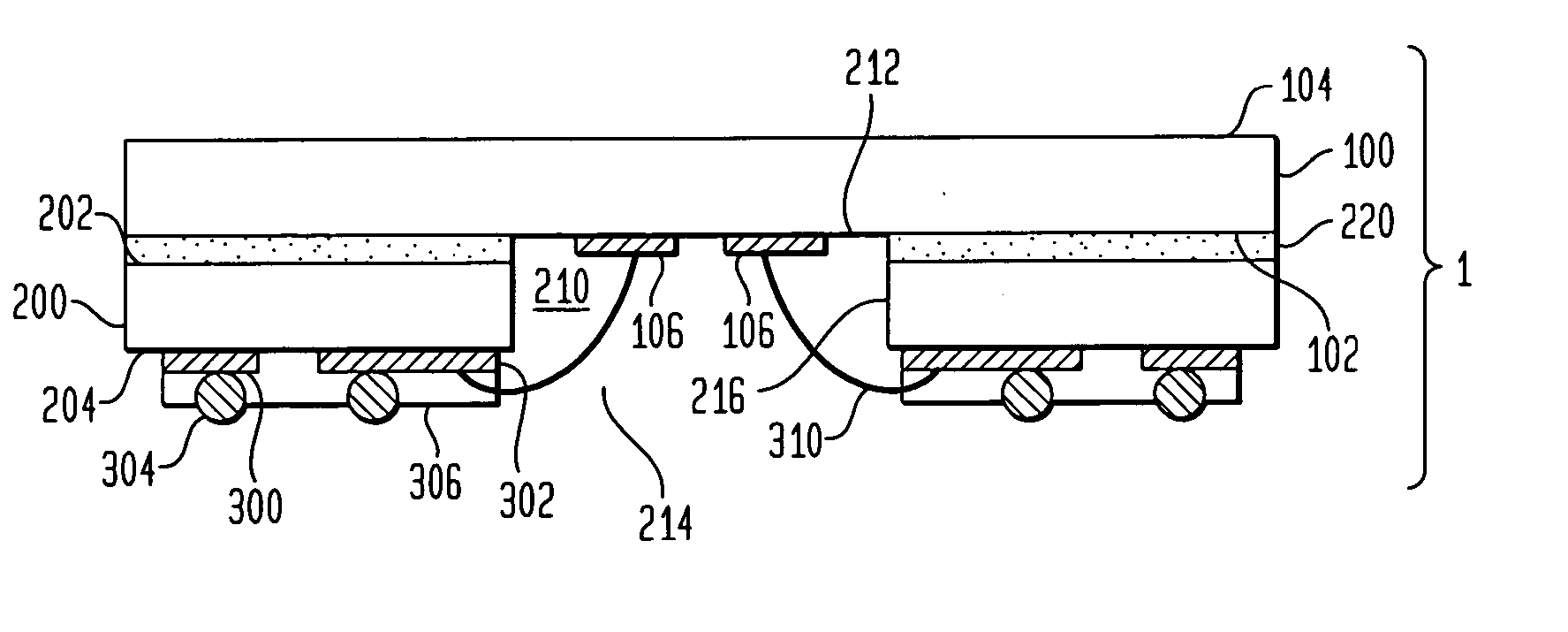
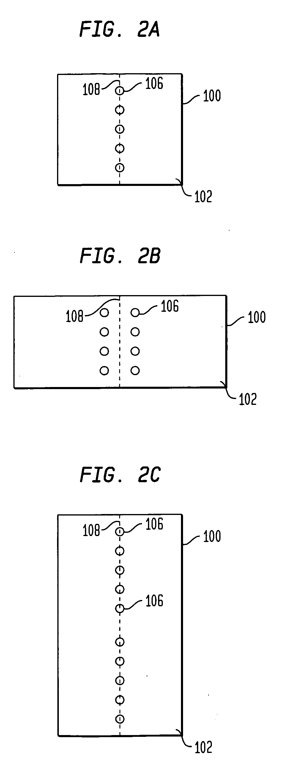
[0028] It is to be understood that the invention is not limited to specific microelectronic devices or types of electronic products, as such may vary. It is also to be understood that the terminology used herein is for the purpose of describing particular embodiments only, and is not intended to be limiting.

[0029] As used in this specification and the appended claims, the singular article forms “a,”“an,” and “the”include both singular and plural referents unless the context clearly dictates otherwise. Thus, for example, reference to“a conductive region,” includes a plurality of conductive regions as well as a single conductive region, reference to “a microelectronic device” includes a single device as well as a combination of devices, and the like.

[0030] In addition, terminology indicative or suggestive of a particular spatial relationship between elements of the invention is to be construed in a relative sense rather an absolute sense unless the context of usage clearly dictates ...


PUM


Abstract

A microelectronic package includes a microelectronic device, a unitary ceramic substrate, and a plurality of terminals. The microelectronic device has a front surface and a plurality of electrical contacts thereon. The substrate has first and second opposing surfaces. A window extends from a first opening on the first surface along a side wall to a second opening on the second surface. A conductive region may be provided on the side wall and / or the second substrate surface. The substrate is located between the device and the terminals such that the first surface of the substrate faces the front surface of the device and the first opening is aligned with at least one contact on the front device surface. Also provided are methods for producing microelectronic packages and wafer-scale assemblies.

Description

BACKGROUND OF THE INVENTION [0001] The invention relates generally to microelectronic packages. In particular, the invention relates to microelectronic packages that employ a ceramic substrate having a conductive surface region, optionally on a window side wall, to which a microelectronic device may be electrically connected. Also provided are wafer-scale microelectronic assemblies and methods for forming microelectronic packages and assemblies. [0002] Microelectronic devices such as semiconductor chips are often packaged with a substrate to provide a convenient vehicle for mounting and electrically connecting the device. For example, semiconductor chips typically are flat bodies with contacts disposed on the front surface that are connected to the internal electrical circuitry of the chip itself. Semiconductor chips are typically packaged with substrates to form microelectronic packages having terminals that are electrically connected to the chip contacts. The package may then be c...

Claims


Application Information

Patent Timeline
Patent Type & Authority Applications(United States)
IPC IPC(8): H01L23/06
CPCH01L23/13H01L23/49816H01L23/49822H01L23/5389H01L2224/48091H01L2224/4824H01L2224/73215H01L2924/01029H01L2924/01046H01L2924/01078H01L2924/01079H01L2924/04941H01L2924/14H01L2924/15311H01L2924/30107H01L2924/00014H01L24/48H01L2924/01322H01L2224/32225H01L2924/00
Inventor LIEW, VICTORHUMPSTON, GILES
Owner TESSERA INC
Why Eureka
Try Eureka