Semiconductor device heat sink package and method

a technology of semiconductor devices and heat sinks, applied in semiconductor devices, semiconductor/solid-state device details, electrical apparatus, etc., can solve problems such as electrical circuit failure, many approaches that do not offer optimal heat dissipation, and adverse effects

Inactive Publication Date: 2005-04-14
DELPHI TECH INC
View PDF6 Cites 51 Cited by
  • Summary
  • Abstract
  • Description
  • Claims
  • Application Information

AI Technical Summary

Problems solved by technology

Excessive heat build-up within certain electronic packages and other components within a module may lead to adverse effects including electrical circuit failure.
While conventional approaches generally suffice to dissipate some of the thermal energy (heat) away from the semiconductor device, many approaches do not offer optimal heat dissipation.
The resultant heat dissipation realized in many conventional semiconductor packages results in size and power limitations.

Method used


Image

  • Semiconductor device heat sink package and method
  • Semiconductor device heat sink package and method
  • Semiconductor device heat sink package and method

Examples


Embodiment Construction

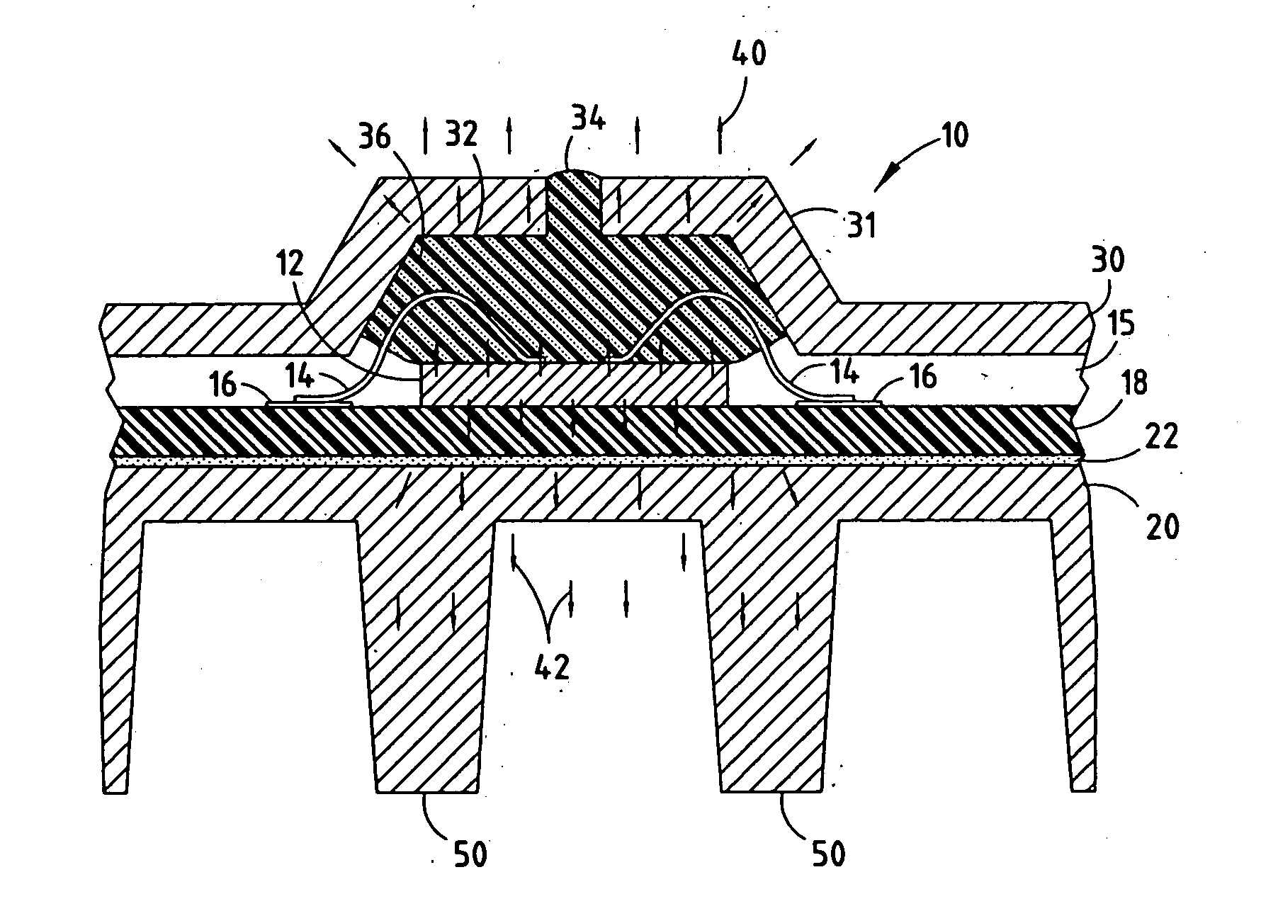
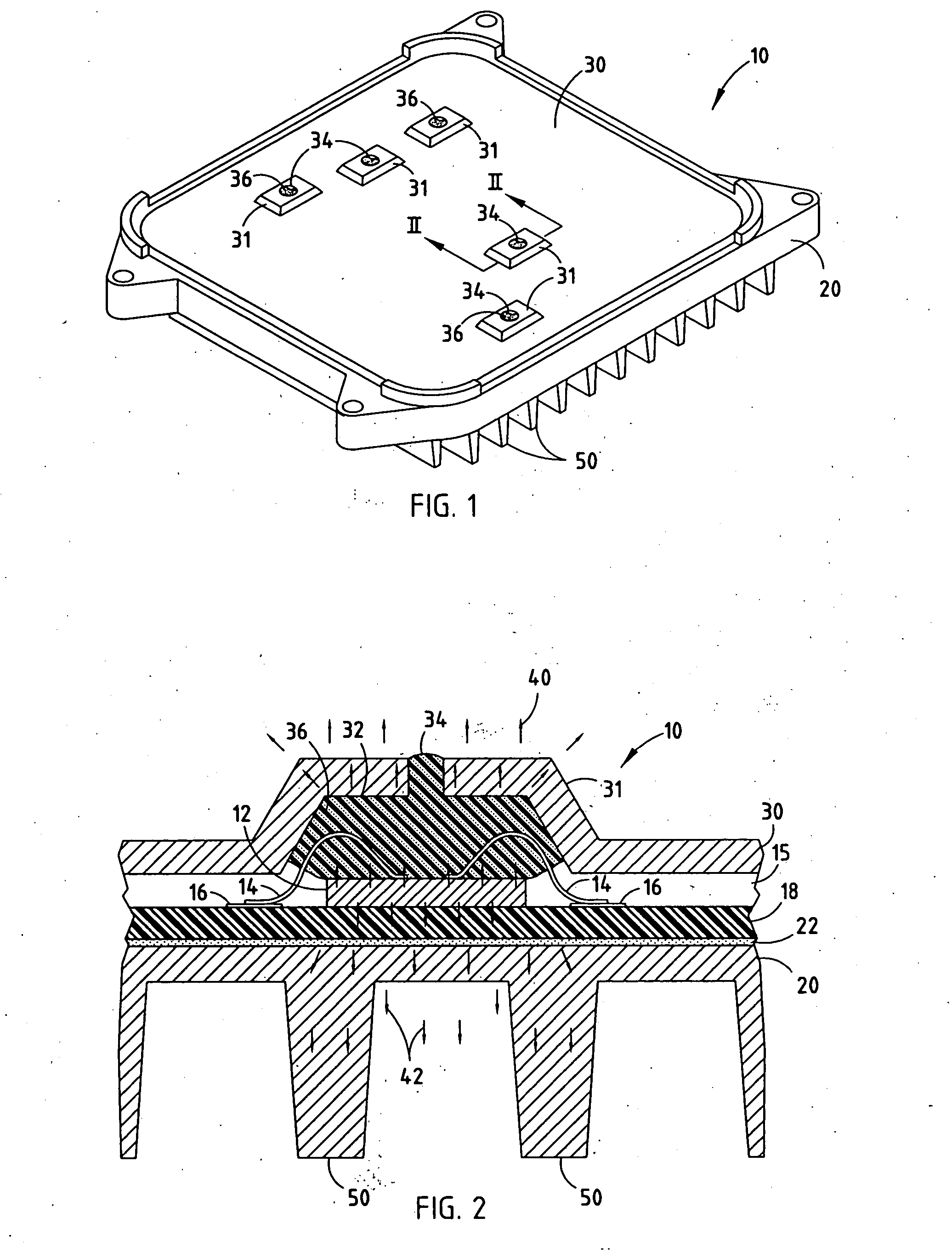
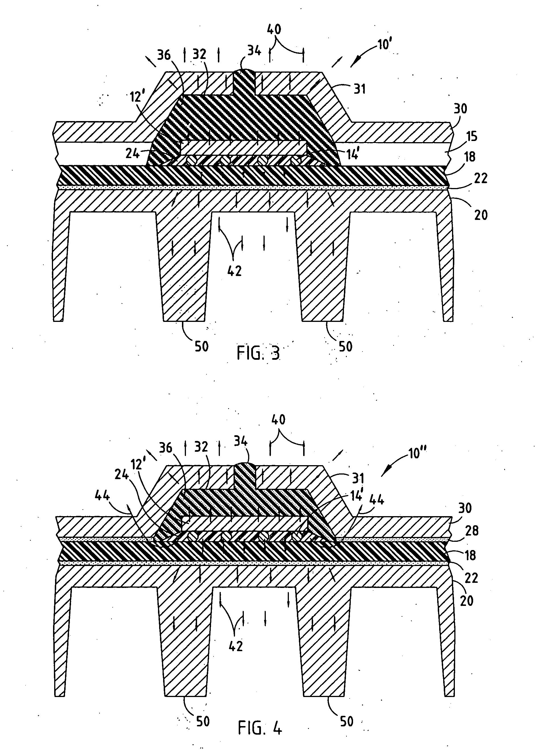
[0015] Referring to FIG. 1, an electronic package 10 is generally illustrated having a lower case 20 and an upper cover 30 forming an enclosure containing electrical circuitry. The electronic package 10 may be employed as an electronic control module (ECM) for use on a vehicle, according to one example. The electronic package 10 has a plurality of semiconductor devices mounted onto one or more circuit boards within the enclosure. In the example shown, the electronic package 10 includes a plurality of semiconductor devices mounted to a substrate; however, it should be appreciated that one or more semiconductor devices may be mounted on one or more substrates and arranged in a thermally (heat) conductive relationship with one or more heat sinks according to the present invention. While the electronic package 10 is shown substantially enclosed, it should be appreciated that package 10 may be otherwise configured with the semiconductor device(s) not enclosed within a surrounding case an...


PUM


Abstract

An electronic package having enhanced heat dissipation is provided exhibiting dual conductive heat paths in opposing directions. The package includes a substrate and a semiconductor device mounted to the substrate. The semiconductor device has electrical circuitry a first surface, and a second surface oppositely disposed from the first surface. A thermally conductive heat sink is assembled over the semiconductor device such that a cavity is formed between the semiconductor device and the heat sink. A thermally conductive and electrically insulative material is disposed in the cavity between the semiconductor device and the heat sink.

Description

CROSS-REFERENCE TO RELATED APPLICATION [0001] This application is related to Application Ser. No. [Docket No. DP-309960], entitled “FLIP CHIP HEAT SINK PACKAGE AND METHOD,” filed on the same date.TECHNICAL FIELD [0002] The present invention generally relates to heat generating semiconductor devices and, more particularly, to a semiconductor device and heat sink assembly for dissipating heat away from the semiconductor device. BACKGROUND OF THE INVENTION [0003] Electronic packages, such as electronic control modules, generally contain fabricated electrical circuitry including electronic components such as transistors and resistors. The circuitry conducts electrical current which, in turn, generates thermal energy (i.e., heat) within the electronic package. Excessive heat build-up within certain electronic packages and other components within a module may lead to adverse effects including electrical circuit failure. Thus, it is desirable to dissipate heat away from the electronic pack...

Claims


Application Information

Patent Timeline
Patent Type & Authority Applications(United States)
IPC IPC(8): H01L23/42H01L25/065
CPCH01L23/42H01L25/0655H01L2924/0002H01L2924/00
Inventor CHENGALVA, SURESH K.SARMA, DWADASI H.R.ZIMMERMAN, DAVID W.MANDEL, LARRY M.GERTISER, KEVIN M.
Owner DELPHI TECH INC
Why Eureka
Try Eureka