Package-on-package assembly with wire bond vias

a technology of wire bonding and packaging, which is applied in the manufacture of printed circuits, printed circuit aspects, basic electric elements, etc., can solve the problems of difficult or impossible to form arrays of microcontacts with appreciable height and very small pitch or spacing, and the configuration of microcontacts formed by conventional etching processes is limited

Active Publication Date: 2013-04-18
INVENSAS LLC
View PDF42 Cites 50 Cited by
  • Summary
  • Abstract
  • Description
  • Claims
  • Application Information

AI Technical Summary

Problems solved by technology

It has been difficult or impossible to form arrays of microcontacts with appreciable height and very small pitch or spacing between adjacent microcontacts.
Moreover, the configurations of the microcontacts formed by conventional etching processes are limited.

Method used


Image

  • Package-on-package assembly with wire bond vias
  • Package-on-package assembly with wire bond vias
  • Package-on-package assembly with wire bond vias

Examples


Embodiment Construction

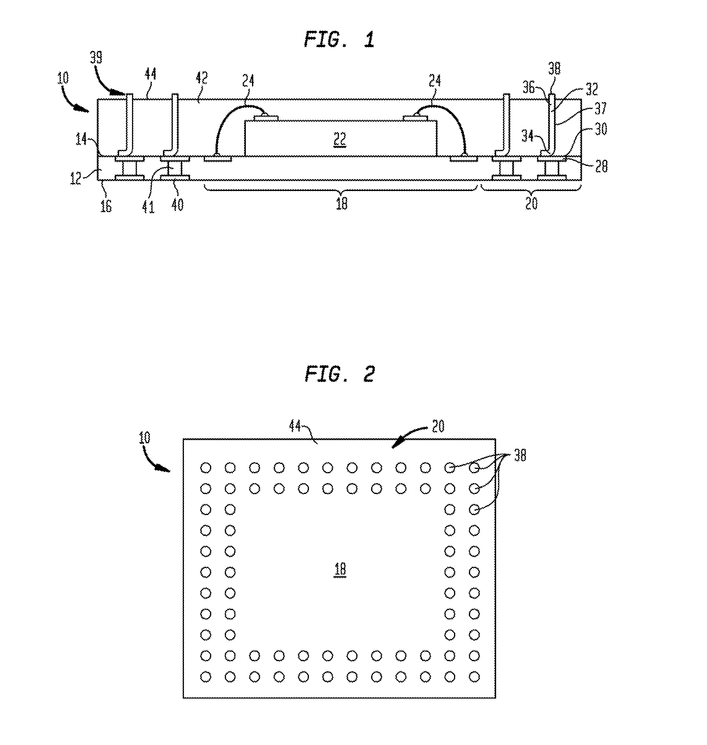
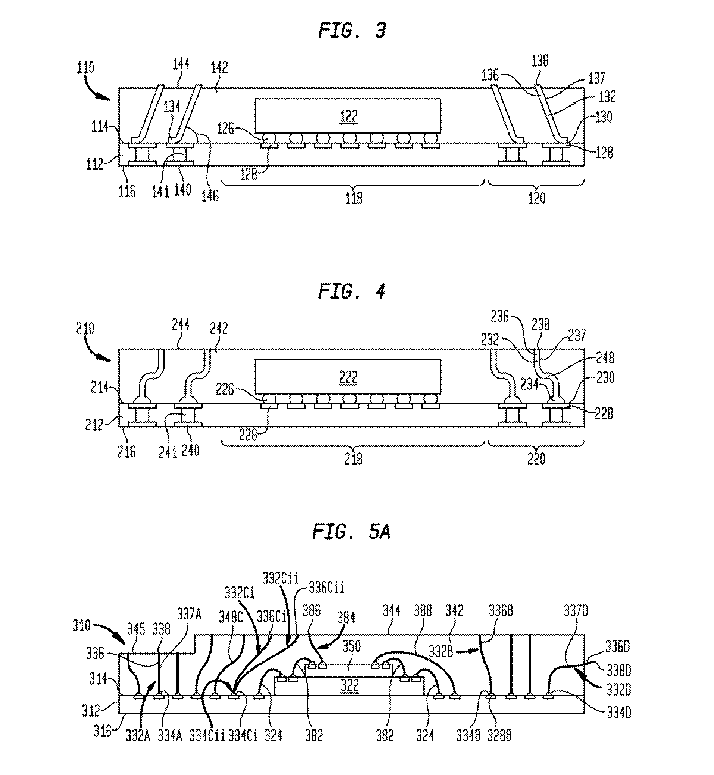
[0079]Turning now to the figures, where similar numeric references are used to indicate similar features, there is shown in FIG. 1 a microelectronic assembly 10 according to an embodiment of the present invention. The embodiment of FIG. 1 is a microelectronic assembly in the form of a packaged microelectronic element such as a semiconductor chip assembly that is used in computer or other electronic applications.

[0080]The microelectronic assembly 10 of FIG. 1 includes a substrate 12 having a first surface 14 and a second surface 16. The substrate 12 typically is in the form of a dielectric element, which is substantially flat. The dielectric element may be sheet-like and may be thin. In particular embodiments, the dielectric element can include one or more layers of organic dielectric material or composite dielectric materials, such as, without limitation: polyimide, polytetrafluoroethylene (“PTFE”), epoxy, epoxy-glass, FR-4, BT resin, thermoplastic, or thermoset plastic materials. T...


PUM

PropertyMeasurementUnit
angleaaaaaaaaaa
angleaaaaaaaaaa
angleaaaaaaaaaa

Abstract

A microelectronic package can include wire bonds having bases bonded to respective ones of conductive elements exposed at a surface of a substrate. The wire bonds may have exterior edge surfaces disposed at an angle between 25° and 92° relative to the bases, and ends remote, e.g., opposite, from the bases, and remote from the ends which are connected to the bases. A dielectric encapsulation layer extends from the substrate and covers portions of the wire bonds such that covered portions of the wire bonds are separated from one another by the encapsulation layer, wherein unencapsulated portions of the wire bonds are defined by portions of the wire bonds that are uncovered by the encapsulation layer, the unencapsulated portions including the ends of the wire bonds.

Description

CROSS-REFERENCE TO RELATED APPLICATIONS[0001]This application claims the benefit of the filing date of U.S. Provisional Application 61 / 547,930 filed Oct. 17, 2011, the disclosure of which is incorporated by reference herein.BACKGROUND OF THE INVENTION[0002]Microelectronic devices such as semiconductor chips typically require many input and output connections to other electronic components. The input and output contacts of a semiconductor chip or other comparable device are generally disposed in grid-like patterns that substantially cover a surface of the device (commonly referred to as an “area array”) or in elongated rows which may extend parallel to and adjacent each edge of the device's front surface, or in the center of the front surface. Typically, devices such as chips must be physically mounted on a substrate such as a printed circuit board, and the contacts of the device must be electrically connected to electrically conductive features of the circuit board.[0003]Semiconduct...

Claims


Application Information

Patent Timeline
Patent Type & Authority Applications(United States)
IPC IPC(8): H01L21/60H01L21/58H01L21/56
CPCH01L23/49517H01L21/4853H01L23/3128H01L23/49811H01L21/56H01L21/565H01L24/16H01L24/48H01L24/49H01L24/73H01L24/78H01L24/85H01L25/0655H01L25/0657H01L25/105H01L25/50H01L2224/16145H01L2224/16225H01L2224/45565H01L2224/48091H01L2224/48145H01L2224/48227H01L2224/4824H01L2224/48245H01L2224/48247H01L2224/49171H01L2224/73204H01L2224/73207H01L2224/73253H01L2224/73257H01L2224/78301H01L2224/8518H01L2224/85951H01L2224/85986H01L2225/0651H01L2225/06517H01L2225/1023H01L2225/1029H01L2225/1052H01L2225/1058H01L2225/1094H01L2924/1431H01L2924/1434H01L2924/15311H01L2924/15331H01L2924/1815H01L2924/19107H01L2225/06513H01L2224/48997H01L2225/06558H01L2225/06506H01L2225/06565H01L2225/06562H01L2225/06568H01L2924/1715H01L2224/32225H01L2224/32245H01L2924/3511H01L2224/32145H01L2224/73265H01L2224/45124H01L2224/45144H01L2224/45147H01L2225/1088H05K3/3436H05K2201/10515H05K2201/1053H01L2924/01013H01L2924/01028H01L2924/01029H01L24/06H01L2224/131H01L23/3677H01L23/4334H01L23/49816H01L2224/16227H01L2924/01047Y10T29/49151Y10T29/49149H01L2224/45664H01L2924/00014H01L2924/00H01L2924/00012H01L2924/014H01L2224/45015H01L2924/181H01L2924/12042H01L2224/0401H01L2224/05599H01L2224/85399H01L24/45H01L2924/00011H01L23/3114H01L2224/4554H01L2924/20751H01L2924/20752H01L2924/20753H01L2924/20754H01L2924/20755H01L2924/20756H01L2924/20757H01L2924/20758H01L2924/20759H01L2924/2076H01L2924/01049H01L24/43H01L2224/851
Inventor CHAU, ELLISCO, REYNALDOALATORRE, ROSEANNDAMBERG, PHILIPWANG, WEI-SHUNYANG, SE YOUNG
Owner INVENSAS LLC
Why Eureka
Try Eureka