Supercharge Your Innovation With Domain-Expert AI Agents!

Electronic device and process for forming same

a technology of electronic devices and processes, applied in the direction of electroluminescent light sources, thermoelectric devices, electric lighting sources, etc., can solve the problems of poor device performance, poor yield in the device fabricating process, and difficult manufacturing of electronic components that include organic active layers

Inactive Publication Date: 2006-07-06
LG CHEM LTD +1
View PDF42 Cites 13 Cited by
  • Summary
  • Abstract
  • Description
  • Claims
  • Application Information

AI Technical Summary

Benefits of technology

[0007] In one exemplary embodiment, an electronic device includes a substrate and a well structure overlying the substrate and defining an array of openings. From a cross-sectional view, the well structure, at the openings has a negative slope. From a plan view, each opening corresponds to an organic electronic component. Each opening within the array of openings has a width and two immediately adjacent openings within the array of openings are connected by a channel having a width less than the width of each opening.

Problems solved by technology

However, the manufacturing of electronic components that include organic active layers is difficult.
Inconsistent formation of organic active layers typically leads to poor device performance and poor yield in device fabricating processes.
In the case of liquid deposition of organic active layers, poor wetting of electrodes may lead to voids within the organic active layer.
When a liquid composition is deposited into a well formed by a surrounding structure, it may form voids.
Such voids decrease the available surface area for radiation emission or radiation absorption, leading to reduced performance.
However, such structures may form breaks in overlying electrode structures, such as cathodes.

Method used


Image

  • Electronic device and process for forming same
  • Electronic device and process for forming same
  • Electronic device and process for forming same

Examples


Embodiment Construction

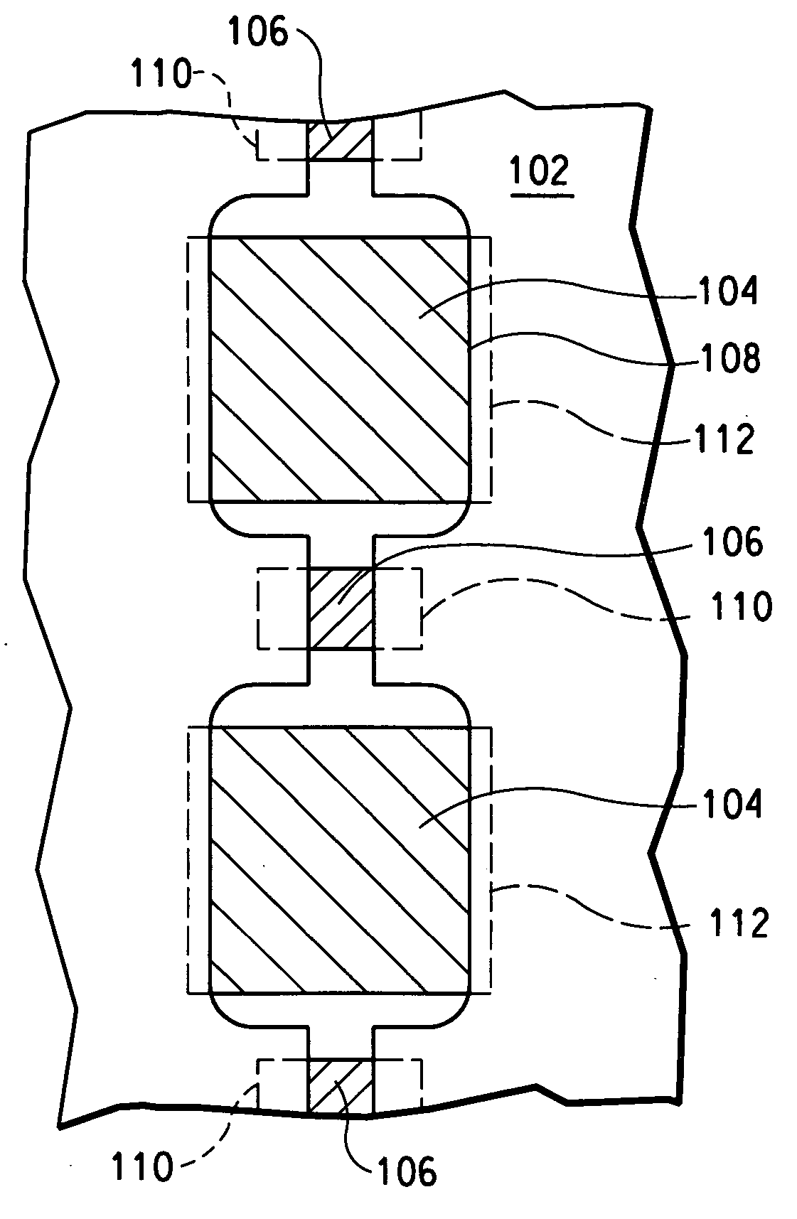
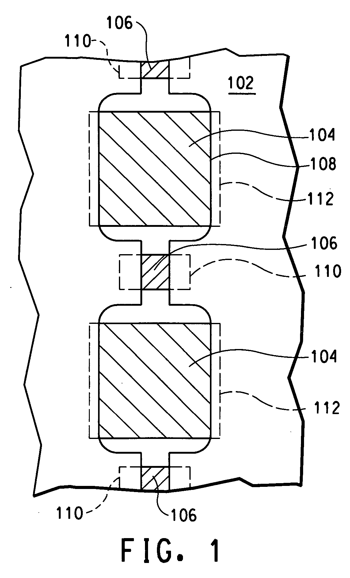
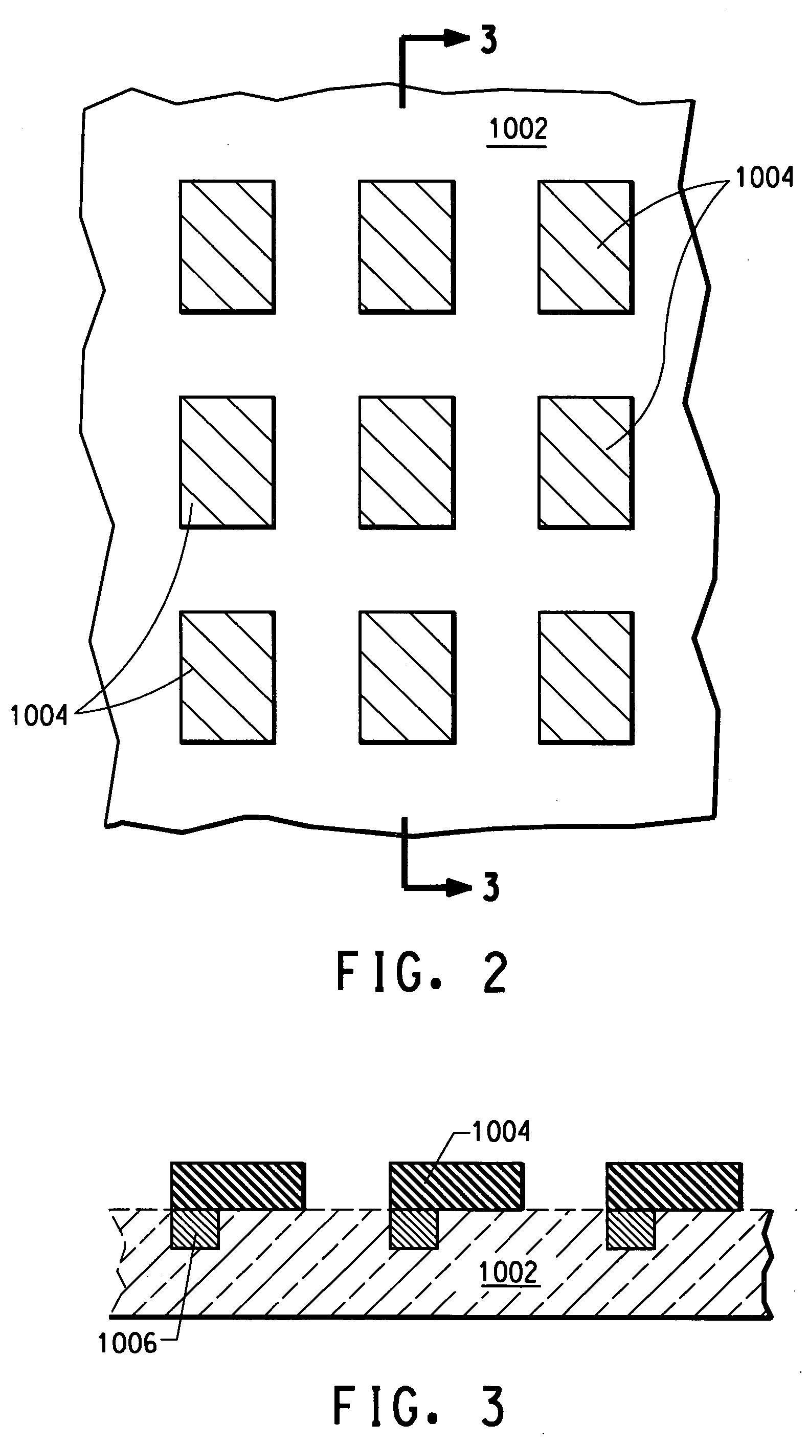
[0019] An electronic device includes a substrate and a well structure overlying the substrate and defining an array of openings. From a cross-sectional view, the well structure, at the openings has a negative slope. From a plan view, each opening corresponds to an organic electronic component. Each opening within the array of openings has a width and two immediately adjacent openings within the array of openings are connected by a channel having a width less than the width of each opening.

[0020] The electronic device may further include an electrode lying within the two immediately adjacent openings and within the channel, wherein the electrode provides a conduction path between the two immediately adjacent openings along the electrode. The electrode may form a conduction path between organic electronic components along a vector of the array of openings.

[0021] In one embodiment, each opening within the array has a length. For example, the length is substantially perpendicular to t...


PUM

PropertyMeasurementUnit
wetting angleaaaaaaaaaa
angleaaaaaaaaaa
angleaaaaaaaaaa

Abstract

An electronic device includes a substrate and a well structure overlying the substrate and defining an array of openings. From a cross-sectional view, the well structure, at the openings has a negative slope. From a plan view, each opening corresponds to an organic electronic component. Each opening within the array of openings has a width and two immediately adjacent openings within the array of openings are connected by a channel having a width smaller than the width of each opening.

Description

FIELD OF THE INVENTION [0001] This invention relates in general to electronic devices and methods for forming electronic devices. More specifically, the invention relates to electronic devices including organic electronic components [0002] This application claims priority to Provisional Application No. 60 / 640,502 filed Dec. 30, 2004. BACKGROUND INFORMATION [0003] Increasingly, active organic molecules are used in electronic devices. These active organic molecules have electronic or electro-radiative properties including electroluminescence. Electronic devices that incorporate organic active materials may be used to convert electrical energy into radiation and may include a light-emitting diode, light-emitting diode display, or diode laser. Electronic devices that incorporate organic active layers may also be used to generate signals in response to radiation (e.g., photodetectors (e.g., photoconductive cells, photoresistors, photoswitches, phototransistors, phototubes), infrared (“IR...

Claims


Application Information

Patent Timeline
Patent Type & Authority Applications(United States)
IPC IPC(8): H01L29/08
CPCH01L27/307H01L27/3246H01L27/3283H01L51/0034H01L51/007H01L51/0037H01L51/0038H01L51/0062H01L51/0035H10K39/32H10K59/173H10K59/122H10K85/10H10K85/111H10K85/1135H10K85/114H10K85/649H10K85/6565H05B33/22H05B33/26H01L29/08H10K39/00
Inventor SORICH, STEPHENSTAINER, MATTHEW
Owner LG CHEM LTD
Features
  • R&D
  • Intellectual Property
  • Life Sciences
  • Materials
  • Tech Scout
  • Unparalleled Data Quality
  • Higher Quality Content
  • 60% Fewer Hallucinations
Learn More