DFN semiconductor package having reduced electrical resistance

Active Publication Date: 2006-07-06
ALPHA & OMEGA SEMICON LTD
View PDF1 Cites 27 Cited by
  • Summary
  • Abstract
  • Description
  • Claims
  • Application Information

AI Technical Summary

Benefits of technology

[0007] In accordance with one aspect of the invention, a DFN semiconductor package includes a leadframe having a die bonding pad formed integrally with a drain lead, a source lead bonding area and a gate lead bonding area, the source lead bonding area and the gate lead bonding area being of increas

Problems solved by technology

QFN and DFN packages of the prior art suffer

Method used


Image

  • DFN semiconductor package having reduced electrical resistance
  • DFN semiconductor package having reduced electrical resistance
  • DFN semiconductor package having reduced electrical resistance

Examples


Example

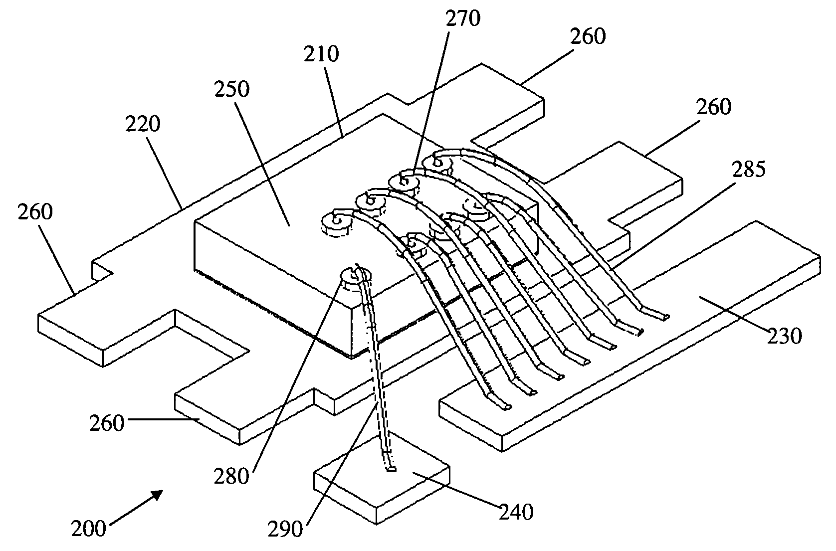
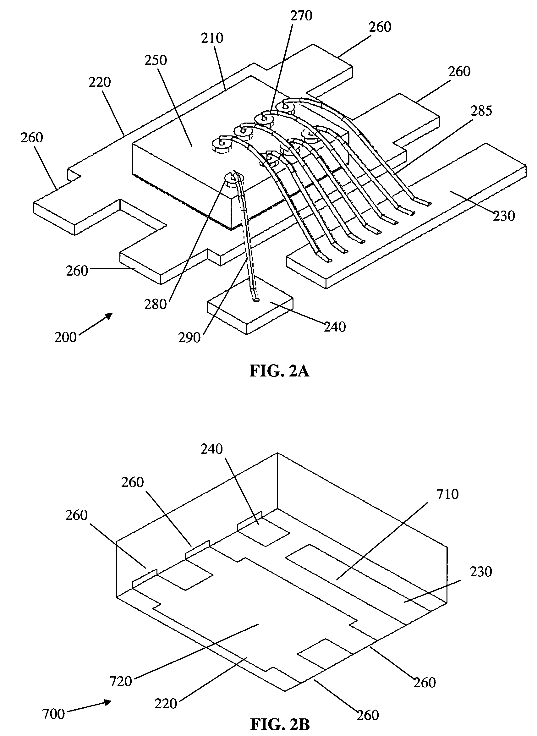
[0031] The present invention generally provides a power MOSFET DFN semiconductor package exhibiting improved electrical characteristics. An increased source bonding area provides for an increased number of source bonding wires having a 2 mil diameter. Improved thermal performance is also provided by an increased contact area between the encapsulant and the source bonding area and source bonding wires.

[0032] In a first aspect of the invention and with reference to FIG. 2A, a DFN semiconductor package generally designated 200 may include a leadframe 210 fabricated of copper, aluminum, nickel or other good electrical and thermal conductive material. Leadframe 210 may be fabricated using metal plating or general manufacturing techniques. Leadframe 210 may include a drain portion 220 fused to drain leads 260, a source portion or lead 230 and a gate portion or lead 240. A power MOSFET die 250 may be attached to a die bonding pad 300 (FIG. 3A). Drain portion 220 may include four drain lea...


PUM


Abstract

A DFN semiconductor package is disclosed. The package includes a leadframe having a die bonding pad formed integrally with a drain lead, a source lead bonding area and a gate lead bonding area, the source lead bonding area and the gate lead bonding area being of increased area, a die coupled to the die bonding pad, a die source bonding area coupled to the source lead bonding area and a die gate bonding area coupled to the gate lead bonding area, and an encapsulant at least partially covering the die, drain lead, gate lead bonding area and source lead bonding area.

Description

CROSS REFERENCE TO RELATED APPLICATION [0001] The present invention is a continuation in part application of commonly assigned Ser. No. 11 / 029,653, filed on Jan. 05, 2005 entitled “Dual Flat Non-Leaded Semiconductor Package”, the disclosure of which is incorporated herein in its entirety.BACKGROUND OF THE INVENTION [0002] The present invention generally relates to semiconductor packages and more particularly to semiconductor packages and methods of making Dual Flat Non-Leaded (DFN) semiconductor packages having reduced electrical resistance and improved thermal properties. [0003] Quad Flat Non-Leaded (QFN) semiconductor packages are well known in the art. QFN semiconductor packages are widely used in high pin out IC package applications. For example, a QFN semiconductor package is disclosed in U.S. Patent Application Publication 2002 / 0177254 entitled “Semiconductor Package and Method for Making the Same”. The disclosed semiconductor package includes a plurality of connection pads an...

Claims


Application Information

Patent Timeline
IPC IPC(8): H01L23/495
CPCH01L23/49562H01L2924/1306H01L24/49H01L24/85H01L2224/32245H01L2224/45144H01L2224/45147H01L2224/48091H01L2224/48095H01L2224/48247H01L2224/48465H01L2224/49111H01L2224/49113H01L2224/49171H01L2224/4943H01L2224/73265H01L2924/01005H01L2924/01013H01L2924/01027H01L2924/01028H01L2924/01029H01L2924/01033H01L2924/01078H01L2924/01079H01L2924/01082H01L2924/13091H01L2924/14H01L2924/30107H01L24/45H01L2224/85H01L2924/014H01L24/48H01L2924/00014H01L2924/00H01L2924/00012H01L2224/45015H01L2924/181H01L2224/0603H01L2224/05553H01L2224/05552
Inventor ZHANG, XIAOTIANLIU, KAISUN, MLNG
Owner ALPHA & OMEGA SEMICON LTD
Why Eureka
Try Eureka