

Flip chip package structure
a chip and package technology, applied in the direction of electrical equipment, semiconductor devices, semiconductor/solid-state device details, etc., can solve the problems of high cost of non-conductive paste b>14/b> used in this method, under-filling material formed by this method often contains air bubbles inside, etc., to increase the reliability of the flip chip package structure and reduce the prime cost
- Summary
- Abstract
- Description
- Claims
- Application Information
AI Technical Summary
Benefits of technology
Problems solved by technology
Method used
Image

Examples
Embodiment Construction
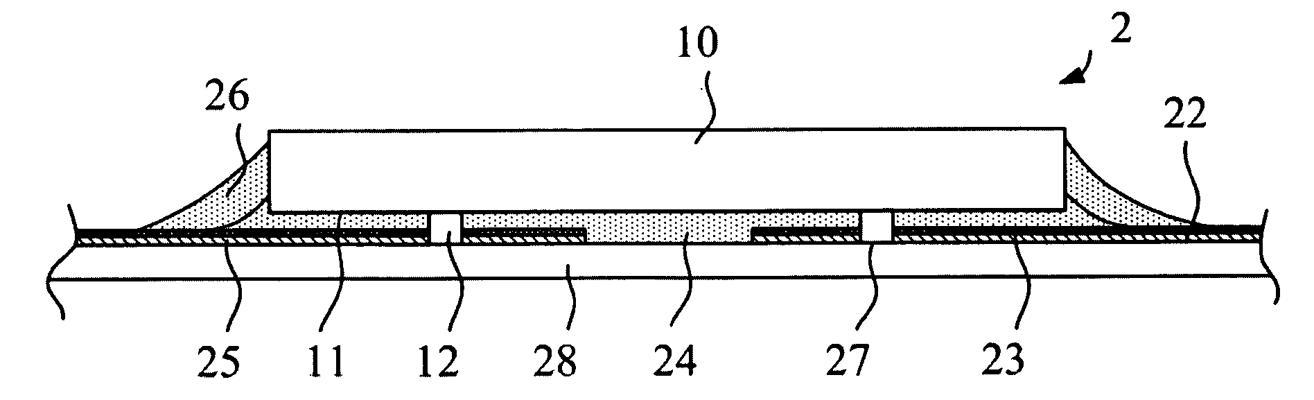
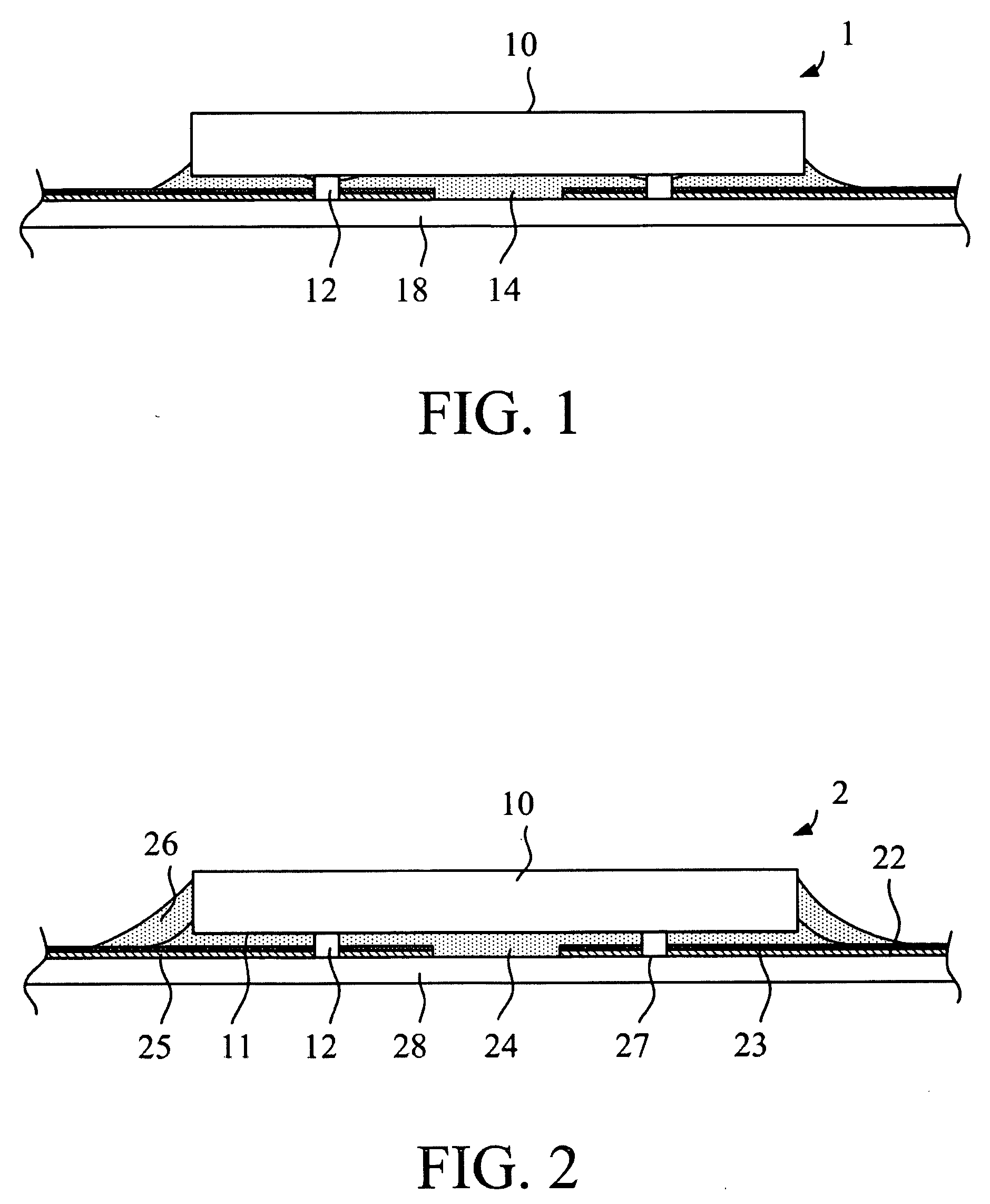
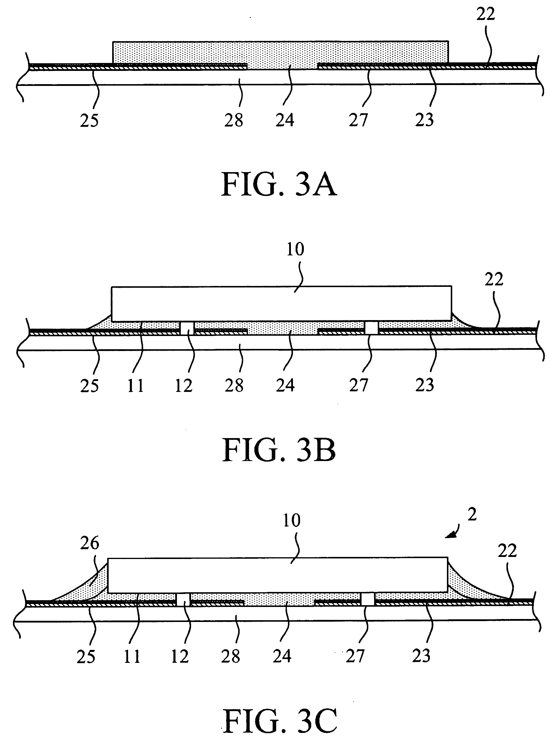
[0016] Please refer to FIG. 2; FIG. 2 is a cross-sectional view showing the flip chip package structure according to the invention. As shown in FIG. 2, the flip chip package structure 2 includes a substrate 28, a flip chip 10, a plurality of bumps 12, a first sealing material 24, and a second sealing material 26. In this embodiment, the substrate 28 is a flexible printing circuit board made of polyimide, polyester or the like. The substrate 28 has an upper surface 22, a plurality of pads 27 formed on the upper surface 22, and a lead layer 25. The lead layer 25 is formed on the upper surface 22 and is connected to the pads 27. An anti-oxidant conductive film 23 is formed on the surface of the pads 27 and the lead layer 25, and it is composed of nickel, aluminum, or tin; consequently, the pads 27 and the lead layer 25 do not have to be covered by a solder mask like the conventional way.
[0017] The flip chip 10 has an active surface 11. In this embodiment, the bumps 12 are gold bumps. ...
PUM
 Abstract
Description
Claims
Application Information