Plasma display panel

a technology of display panels and plasma, applied in the direction of gas mixture absorption, electric discharge tubes, gas-filled discharge tubes, etc., can solve the problems of uneven display, insufficient removal, and discharge characteristic or luminance degradation, and achieve the effect of suppressing the degradation of phosphor luminan

Inactive Publication Date: 2006-07-13
PANASONIC CORP
View PDF8 Cites 5 Cited by
  • Summary
  • Abstract
  • Description
  • Claims
  • Application Information

AI Technical Summary

Benefits of technology

[0012] With this configuration, the non-evaporating getter, a gas adsorption layer, adsorbs impurity gases inside the PDP or those that come in from outside, enabling suppression of phosphor luminance degradation due to impurity gases.

Problems solved by technology

These gases are adsorbed onto the phosphors inside the PDP and cause problems such as degraded discharge characteristic or reduced luminance.
Accordingly, the reduction of impurity gases inside the PDP to stabilize the discharge characteristic and suppress secular change to improve reliability is an important challenge in PDP manufacture.
Since impurity gases exhausted from the PDP are adsorbed onto the inner wall of the exhaust pipe, impurity gases re-enter the PDP together with the discharge gas when feeding in the discharge gas, resulting in their insufficient removal.
Partially remaining impurity gases causes uneven display.
With the method of removing impurity gases by providing a getter inside the exhaust pipe, impurity constituents are gradually accumulated on the getter, and thus its capability to remove impurity gases declines over a period.

Method used


Image

  • Plasma display panel
  • Plasma display panel
  • Plasma display panel

Examples


first exemplary embodiment

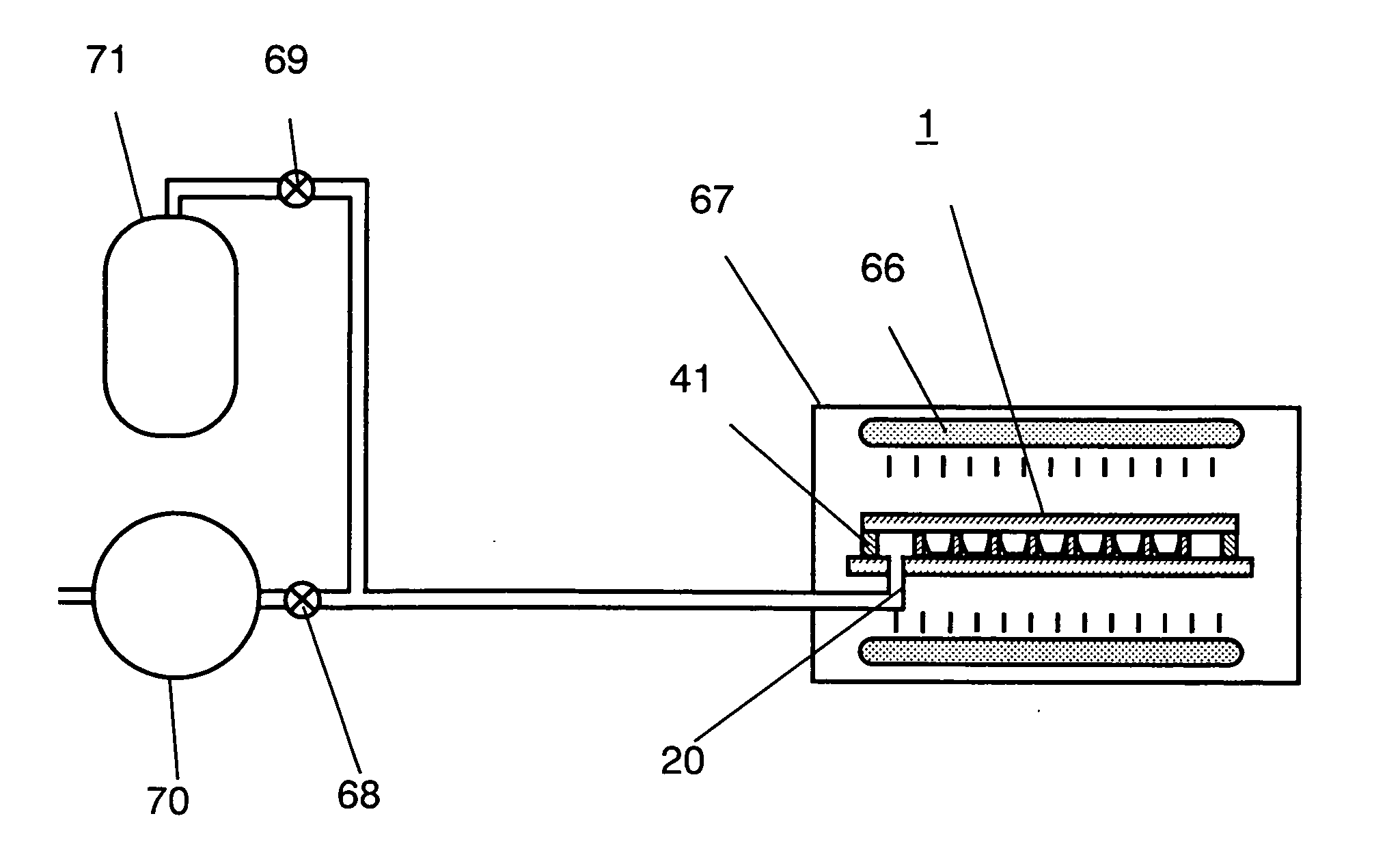
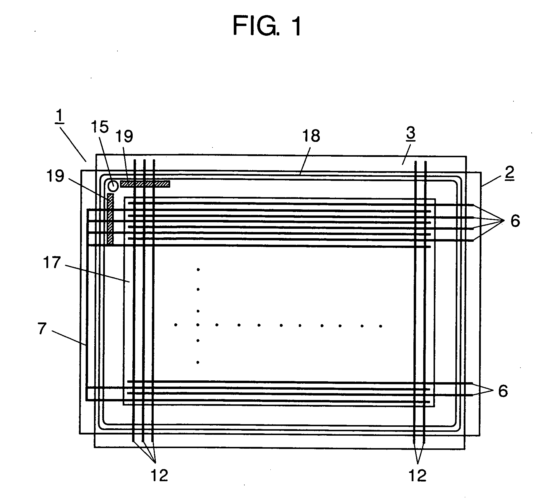
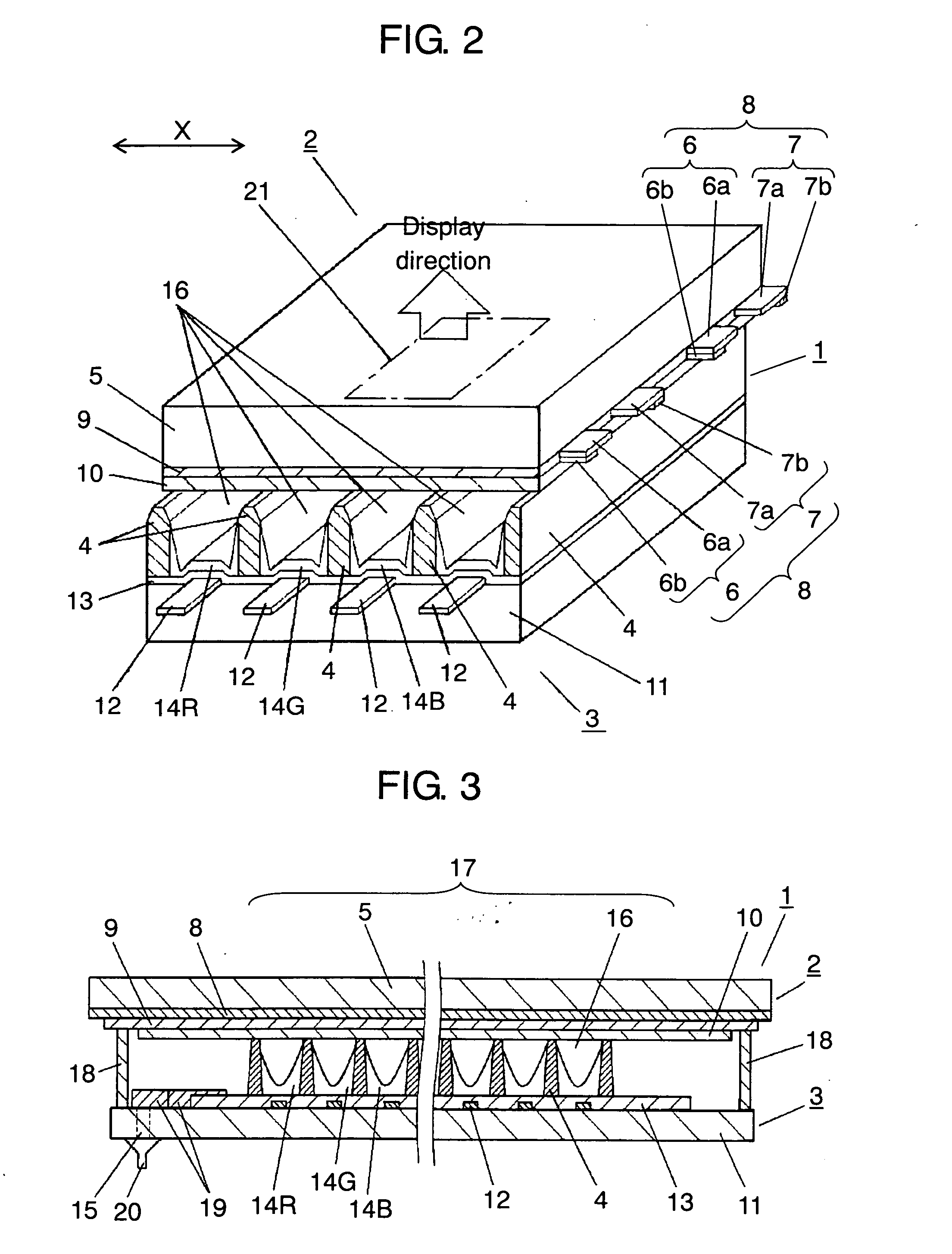
[0020]FIG. 1 is a plan view illustrating a schematic structure of a PDP in a first exemplary embodiment of the present invention. FIG. 2 is a sectional perspective view illustrating a schematic structure of a part of image display area in the PDP in the first exemplary embodiment of the present invention. FIG. 3 is a sectional view illustrating a schematic structure of the PDP in the first exemplary embodiment, taken along direction X in FIG. 2.

[0021] PDP 1 is configured by sandwiching partition 4 between a pair of front board 2 and rear board 3. Front board 2 has display electrode 8, including scanning electrode 6 and maintenance electrode 7 formed on one main face of front glass substrate 5, dielectric layer 9 covering display electrode 8, and protective layer 10 made typically of MgO covering dielectric layer 9. Scanning electrode 6 and maintenance electrode 7 are configured by laminating bus electrodes 6b and 7b onto transparent electrodes 6a and 7a.

[0022] Rear board 3 has dat...

second exemplary embodiment

[0036]FIG. 5 is a plan view of rear board 3 of PDP 1 in a second exemplary embodiment of the present invention. In this exemplary embodiment, zeolite, which acts as non-evaporating getter 19, is applied over the entire periphery of non-image display area 30 between image display area 17 and sealing material 18.

[0037] This configuration increases the adsorption area of zeolite, enhancing the effect of removal of impurity gases.

[0038] Provision of the non-evaporating getter inside the PDP as described above is selectable, and is easily provided by applying paste containing zeolite to predetermined portions in non-image display rear 30.


PUM


Abstract

A highly reliable plasma display panel which suppresses degradation of phosphor characteristic by removing impurity gases inside the plasma display panel. A front board includes scanning electrodes and maintenance electrodes. A and rear board includes data electrodes; partitions disposed in parallel and an exhaust hole. The scanning electrodes and maintenance electrodes of the front board and the data electrode of rear board cross. A non-evaporating getter such as zeolite is disposed inside plasma display panel near the exhaust hole.

Description

TECHNICAL FIELD [0001] The present invention relates to plasma display panels, and more particularly to plasma display panels with stable discharge and stable phosphor characteristics. BACKGROUND ART [0002] In the field of color display devices for images, such as computers and television sets, plasma display devices employing a plasma display panel (PDP) are being increasingly drawing attention due to their advantages of being large, thin and light. [0003] In a PDP, a front board and a rear board are sealed together with a discharge space of predetermined thickness in between. The electrodes and dielectric layer, or partition and phosphor layer, are formed on the front board and rear board respectively by firing structural materials containing organic binder. [0004] During PDP manufacture, impurity gases spread in the PDP by thermal decomposition, typically of the organic binder contained in the glass frit used as sealing material in the sealing process, in particular, that for sea...

Claims


Application Information

Patent Timeline
Patent Type & Authority Applications(United States)
IPC IPC(8): H01J17/49H01J17/24
CPCH01J11/12H01J11/52
Inventor HASEGAWA, KAZUYAKADO, HIROYUKISASAKI, YOSHIKINISHINAKA, MASAKIOKAWA, MASAFUMI
Owner PANASONIC CORP
Why Eureka
Try Eureka