Transfer system and transfer method of object to be processed

Inactive Publication Date: 2006-07-13
TOKYO ELECTRON LTD
View PDF15 Cites 6 Cited by
  • Summary
  • Abstract
  • Description
  • Claims
  • Application Information

AI Technical Summary

Benefits of technology

[0010] It is, therefore, an object of the present invention to provide a transfer system and method for transferring objects to be processed capable of enhancing a transfer efficiency between an automatic transfer device and a processing equipment to thereby reduce a TAT of t

Problems solved by technology

However, in case of a large diameter wafer of, e.g., a 300 mm wafer, the carrier accommodating therein a plurality of wafers is very heavy, thereby making it very difficult for the operator to carry such a carrier.
Meanwhile, with a recent trend towards a large diameter of the wafer and an ultra miniaturization of devices, the number of devices formed on a single wafer is significantly increased, so that much time is needed to complete a processing such as an inspection for a single wafer.
For the reason, although the wafers of a same lot in a carrier can be transferred to a semiconductor manufacturing device such as an inspection device by using the automatic transfer carriage as described above, it takes considerably long time to process all the wafers in the carrier, and even wafers already processed have to stay in the semiconductor manufacturing device during such a process

Method used


Image

  • Transfer system and transfer method of object to be processed
  • Transfer system and transfer method of object to be processed
  • Transfer system and transfer method of object to be processed

Examples


Example

[0038] Hereinafter, preferred embodiments of the present invention will be described with reference to the accompanying drawings.

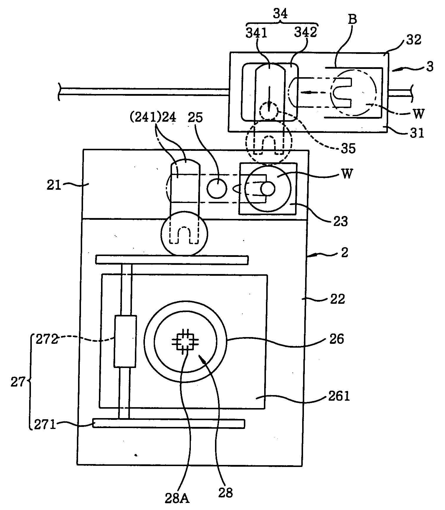
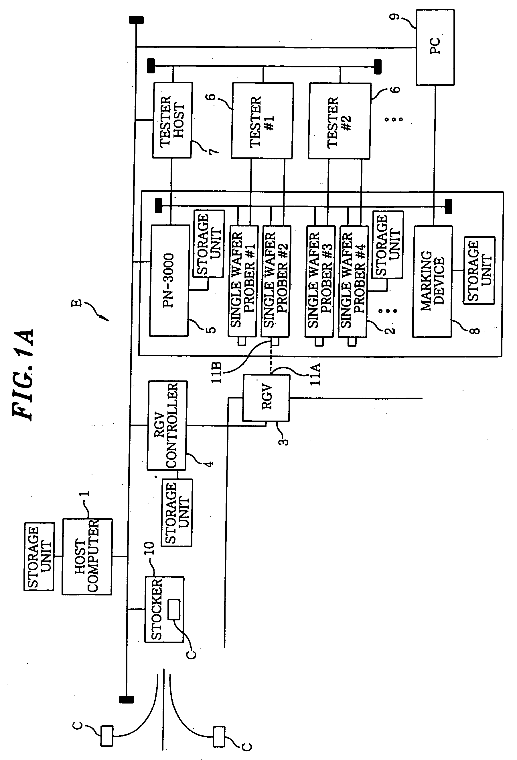
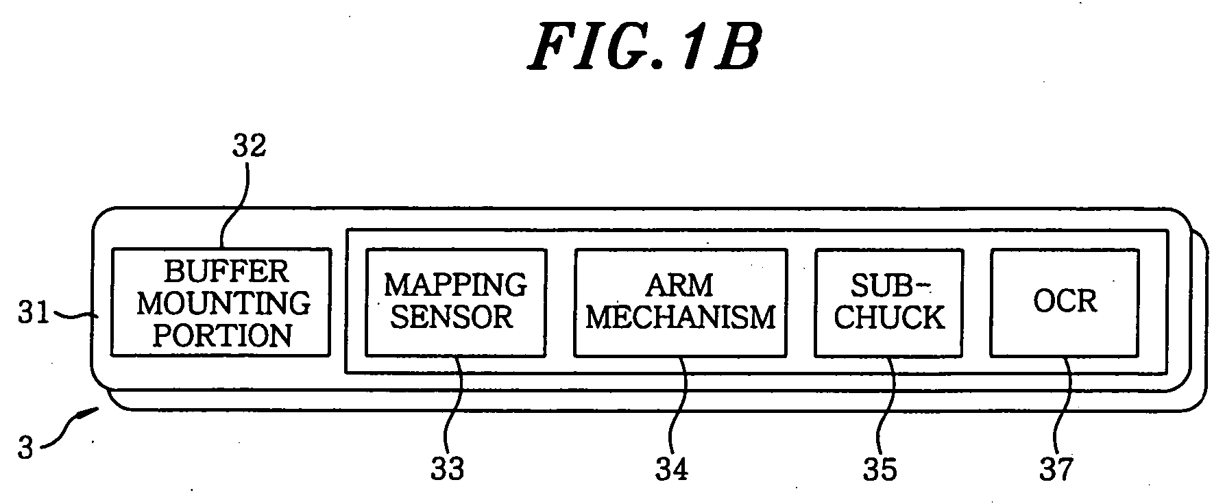
[0039] As shown in FIGS. 1A and 1B, an Automated Material Handling System (AMHS) E for transferring objects to be processed in accordance with a first embodiment of the present invention includes a host computer 1 for managing an overall factory production process containing an inspection process for wafers (not shown) as the objects to be processed; a plurality of probers 2 as an inspection device for inspecting electrical characteristics of the wafers under the management of the host computer 1; a plurality of automatic transfer devices (hereinafter, referred to as “RGV”) for automatically transferring the wafers to the probers 2 one by one in response to respective demands, and a transfer control device (hereinafter, referred to as “RGV controller”) for controlling the RGV's 3. The probers 2 and the RGV's 3 include optically coupled parallel I / O (herei...


PUM


Abstract

A transfer method employs a transfer system including a semiconductor handling device and an automatic transfer device. The semiconductor handling device includes a first transfer mechanism and a first optically coupled parallel I/O communications interface. The automatic transfer device includes a second transfer mechanism and a second optically coupled parallel I/O communications interface. The transfer method includes a successive transfer notifying step wherein the automatic transfer device and the semiconductor handling device notify each other that a successive transfer is possible via an optical communications between the first and the second optically coupled parallel I/O communications interface in case where a plurality of objects to be processed are able to be successively transferred one by one between the first and the second transfer mechanism; and a successive transfer step wherein the objects are transferred one by one between the first and the second transfer mechanism.

Description

[0001] This application is a Continuation Application of PCT International Application No. PCT / JP04 / 013537 filed on Sep. 16, 2004, which designated the United States.FIELD OF THE INVENTION [0002] The present invention relates to a system and a method for transferring objects to be processed; and more particularly, to a system and method for transferring objects to be processed capable of enhancing a transfer efficiency per a single wafer. BACKGROUND OF THE INVENTION [0003] For example, in an inspection process for semiconductor devices, a prober has been widely used as a device for inspecting semiconductor wafers (hereinafter, simply referred to as “wafers”). Generally, the prober includes a loader chamber and a prober chamber to inspect electrical characteristics of the wafers. [0004] The loader chamber has a carrier mounting unit for mounting thereon a carrier accommodating therein a plurality of wafers (e.g., 25 wafers), a wafer transfer mechanism (hereinafter, referred to as “ar...

Claims


Application Information

Patent Timeline
IPC IPC(8): G01R31/28G05B19/02H01L21/00H01L21/677H01L21/68
CPCG01R31/2893G05B19/41815G05B2219/31002G05B2219/31216G05B2219/33198G05B2219/45031H01L21/67265H01L21/67736Y10S414/135Y02P90/02H01L21/67742H01L21/67745H01L21/68707
Inventor IIJIMA, TOSHIHIKOSHIMIZU, SHINYAISHIHARA, KAORI
Owner TOKYO ELECTRON LTD
Why Eureka
Try Eureka