
Thin film transistor panel and liquid crystal display using the same

a thin film transistor and liquid crystal display technology, applied in static indicating devices, instruments, non-linear optics, etc., can solve the problems of limited power supply capacity of batteries used as power sources in mobile technologies, such as portable phones, and achieve the effect of low power consumption

Active Publication Date: 2006-07-20
SAMSUNG DISPLAY CO LTD
View PDF4 Cites 36 Cited by
  • Summary
  • Abstract
  • Description
  • Claims
  • Application Information

AI Technical Summary

Benefits of technology

[0009] Embodiments of the present invention provide a low power-consumption LCD, and an LCD having a display region capable of displaying images at all times, regardless of the operation state of a backlight employed in the LCD.

Problems solved by technology

Power consumption by the backlight represents a large part of the total power consumption of the LCD.
Batteries used as a power source in mobile technologies, such as, for example, portable phones, have limited power supply capacities.

Method used


Image

  • Thin film transistor panel and liquid crystal display using the same
  • Thin film transistor panel and liquid crystal display using the same
  • Thin film transistor panel and liquid crystal display using the same

Examples


Embodiment Construction

[0062] Preferred embodiments of the present invention will be described more fully hereinafter with reference to the accompanying drawings. The present invention may, however, be embodied in different forms and should not be construed as being limited to the embodiments set forth herein.

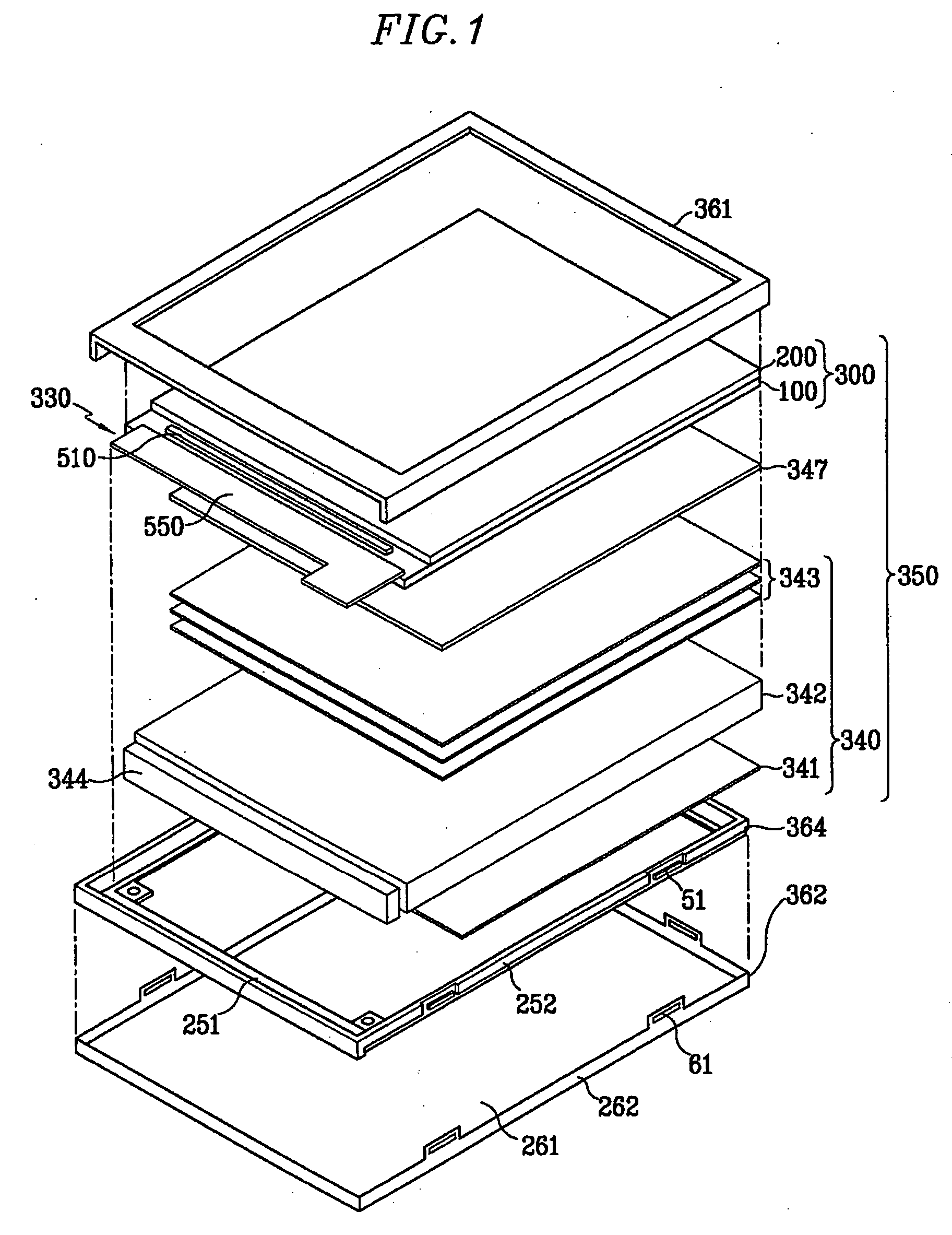
[0063]FIG. 1 is an exploded perspective view schematically illustrating an LCD according to an embodiment of the present invention.

[0064] Referring to FIG. 1, an LCD according to an embodiment of the present invention includes an LC panel assembly 330 for displaying images using light, a backlight assembly 340 for producing light, a selective reflection film 347 provided between the LC panel assembly 330 and the backlight assembly 340, a mold frame 364 for receiving the LC panel assembly 330, the selective reflection film 347, and the backlight assembly 340 therein, and an upper chassis 361 and a lower chassis 362 that surround and support the above-mentioned elements.

[0065] The LC panel assembly ...


PUM


Abstract

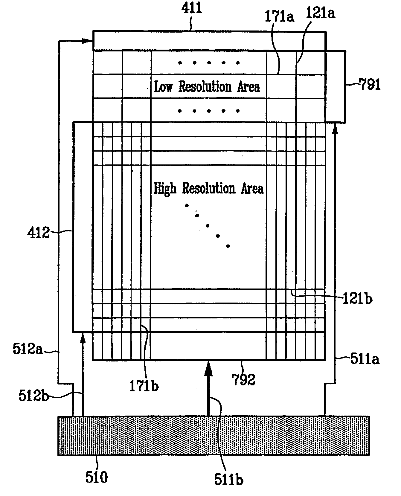
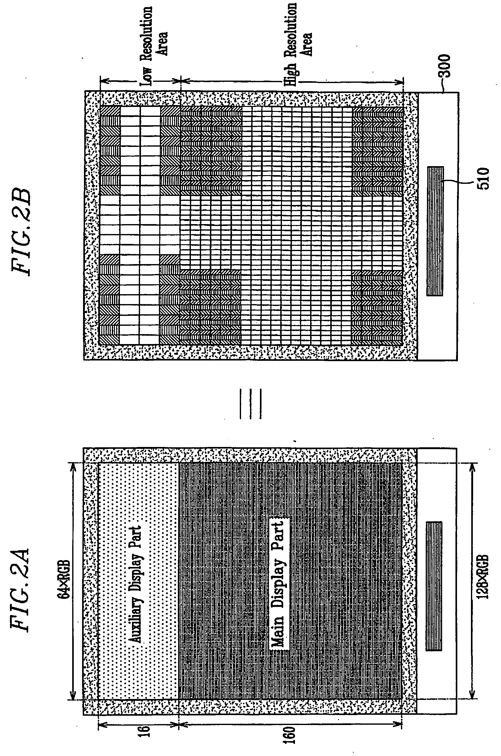
An LCD device includes a transmissive LCD panel assembly, a backlight assembly for supplying light to the LCD panel assembly, and a selective reflection film provided between the backlight assembly and the LCD panel assembly. A display region of the LCD has a low-resolution area and a high-resolution area, and a pixel formed in the low-resolution area that is larger than a pixel formed in the high-resolution area.

Description

BACKGROUND OF THE INVENTION [0001] (a) Technical Field [0002] The present disclosure relates to a liquid crystal display (LCD) and a thin film transistor (TFT) panel for the same. [0003] (b) Discussion of the Related Art [0004] Generally, an LCD includes a pair of panels respectively having electrodes on their inner surfaces, and a dielectric anisotropy liquid crystal layer interposed between the panels. In the LCD, a variation of the voltage difference between the field generating electrodes, i.e., a variation in the strength of an electric field generated by the electrodes, changes the transmittance of the light passing through the liquid crystal layer, and thus desired images are obtained by controlling the voltage difference between the electrodes. [0005] In the LCD, the light may be a natural light or an artificial light emitted from a light source employed in the LCD. [0006] A backlight is a representative device for providing the artificial light in the LCD and utilizes, for ...

Claims


Application Information

Patent Timeline
IPC IPC(8): G02F1/1335
CPCG02F1/1333G02F1/133514G02F1/133555G02F1/133615G02F1/13439G02F1/136286G02F2001/133317G02F2001/133391G02F1/133317G02F1/133391
Inventor UH, KEE-HANKIM, HYUNG-GUELKIM, SANG-WOOLEE, SEUNG-KYUAN, BO-YOUNGPARK, WON-SANGKIM, JAE-HYUNYUN, HAE-YOUNGLEE, JAE-YOUNGIRINA, POUNDALEVACHA, SUNG-EUNCHANG, YOUNG-JOOLIM, JAE-LKJEONG, KI-HUN
Owner SAMSUNG DISPLAY CO LTD
Learn More