Back-contacted solar cells with integral conductive vias and method of making

a solar cell and integral technology, applied in the field of back contact solar cells, can solve the problem of photocurrent loss in heavily doped emitters

Inactive Publication Date: 2006-07-27
ADVENT SOLAR INC
View PDF99 Cites 101 Cited by
  • Summary
  • Abstract
  • Description
  • Claims
  • Application Information

AI Technical Summary

Benefits of technology

[0019] Yet another advantage of the present invention is that n++ conductive vias including a n++ doped trail are formed in the p-type semiconductor substrate, such as a silicon structure

Problems solved by technology

Some photocurrent is lost in heavily doped emitters

Method used


Image

  • Back-contacted solar cells with integral conductive vias and method of making
  • Back-contacted solar cells with integral conductive vias and method of making
  • Back-contacted solar cells with integral conductive vias and method of making

Examples


Embodiment Construction

[0027] Note that in the drawings, the thicknesses of the various layers of insulating, semiconducting, and metallic materials, and other dimensions, such as the width of contact pads, are not drawn to scale, but rather are shown schematically for purposes of illustration and easy identification.

[0028] In the specification and claims, processes referred to as “thermomigration” include any gradient-driven migration process, including thermomigration and electromigration.

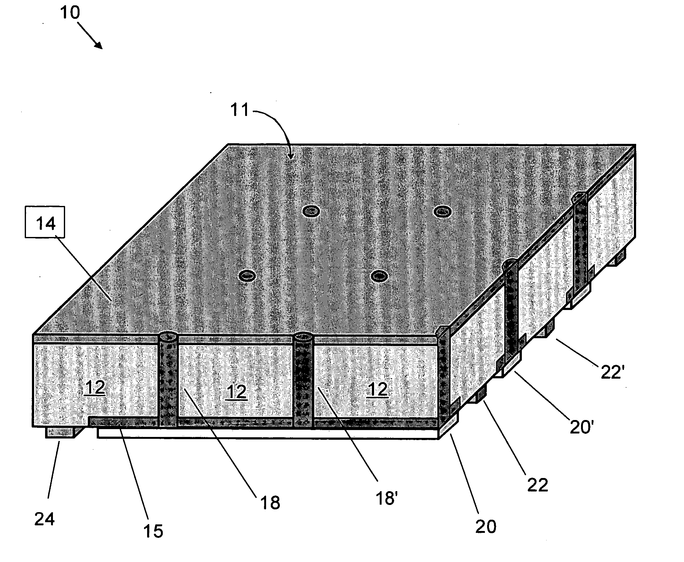
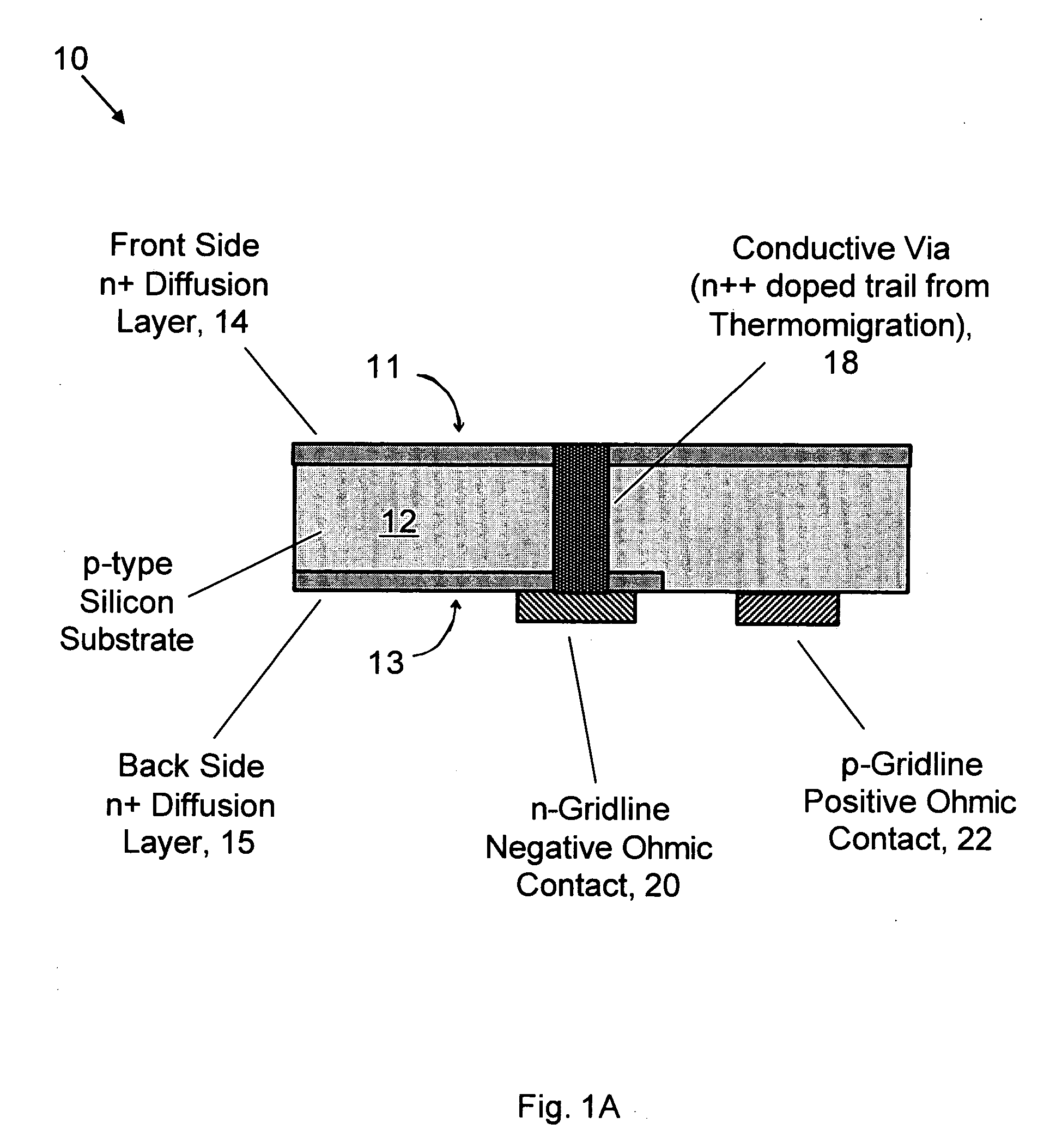
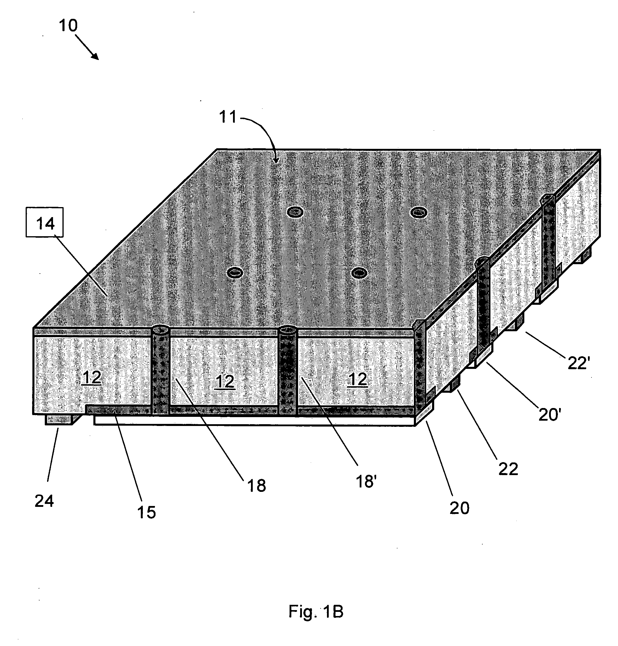
[0029]FIG. 1A shows a schematic cross-section side view of a first example of a back-contacted silicon solar cell, according to the present invention. Back-contacted solar cell 10 comprises a p-type bulk silicon substrate 12; a front side n+ diffusion emitter layer 14 located on the front side 11 of substrate 12; a back side n+ diffusion emitter layer 15 located on the back side 13 of substrate 12; a n-gridline negative ohmic contact 20 located on the back side 13 of substrate 12, contacting back side emitter layer 1...


PUM


Abstract

Methods of manufacturing back-contacted p-type semiconductor substrate solar cells fabricated using a gradient-driven solute transport process, such as thermomigration or electromigration, to create n-type conductive vias connecting the n-type emitter layer on the front side to n-type ohmic contacts located on the back side, and back-contacted solar cells with integral n-type conductive vias, such as made by a gradient-driven solute transport process.

Description

CROSS-REFERENCE TO RELATED APPLICATIONS [0001] This application is a continuation-in-part application of U.S. patent application Ser. No. 10 / 606,487, entitled “Fabrication of Back-Contacted Silicon Solar Cells Using Thermomigration to Create Conductive Vias”, to Gee, et al., filed on Jun. 26, 2003, and a continuation application of International Patent Application Serial No. PCT / US2004 / 020370, entitled “Back-Contacted Solar Cells With Integral Conductive Vias And Method Of Making”, to Gee, et al., filed on Jun. 24, 2004, and the specifications thereof are incorporated herein by reference.FEDERALLY SPONSORED RESEARCH [0002] The United States Government has rights in this invention pursuant to Department of Energy Contract No. DE-AC04-94AL85000 with Sandia Corporation.BACKGROUND OF THE INVENTION [0003] The present invention relates generally to photovoltaic solar cells and methods of making photovoltaic solar cells, and more specifically to back-contacted solar cells with an array of ...

Claims


Application Information

Patent Timeline
IPC IPC(8): H01L31/00H01L21/768H01L31/0224H01L31/04H01L31/05H01L31/068H01L31/18
CPCH01L21/76898Y02E10/50H01L31/022458Y02E10/547
Inventor GEE, JAMES M.SCHMIT, RUSSELL R.
Owner ADVENT SOLAR INC
Why Eureka
Try Eureka