Semiconductor mounting board

a technology of semiconductor mounting board and semiconductor, which is applied in the direction of semiconductor/solid-state device details, instruments, photomechanical equipment, etc., to achieve the effects of reducing the number of soldering holes

Active Publication Date: 2006-07-27
IBIDEN CO LTD
View PDF15 Cites 90 Cited by
  • Summary
  • Abstract
  • Description
  • Claims
  • Application Information

AI Technical Summary

Benefits of technology

[0013] In the semiconductor mounting board of the invention, the thickness of the interposer is preferably set to 0.1 to 0.8 times (more preferably 0.2 to 0.4) the thickness of the printed wiring board having the core substrate and the build-up layers. With this thickness of the interposer, the durability in a heat cycle test with a semiconductor being mounted on the semiconductor mounting board is improved further.
[0014] In the semiconductor mounting board of the invention, the external pads may be the pads formed at the outermost surrounding array of the pad set. In this case, the joining reliability of the portions where the pads of the outermost surrounding array are joined to the interposer, which are the portions that receive the greatest shearing stress, can be improved.
[0015] In the semiconductor mounting board of the invention, the pad set may include pads arranged in at least 30 by 30 square pattern, and the external pads may be the pads included in an area from a first surrounding array to an n-th surrounding array (where n is an integer from 2 to 10), with the first surrounding array being the outermost surrounding array of the pad set. In this case, the joining reliability of the portions where the pads near the outermost surrounding array are joined to the interposer, which are the portions that receive comparatively high shearing stress, can be improved.

Problems solved by technology

Though in this case, voids and angled portions may be formed when the internal pads and the interposer are joined by solder or other joining material, since the shearing stress that is applied to the joining portions of the internal pads is low in comparison the shearing stress applied to the joining portions of the external pads, breakage will not occur readily.

Method used


Image

  • Semiconductor mounting board
  • Semiconductor mounting board
  • Semiconductor mounting board

Examples


examples

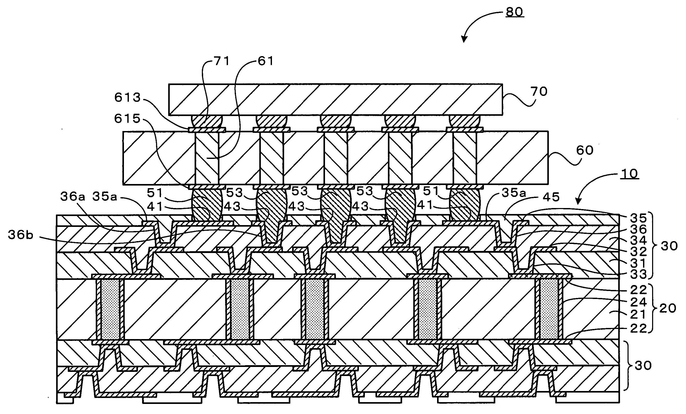
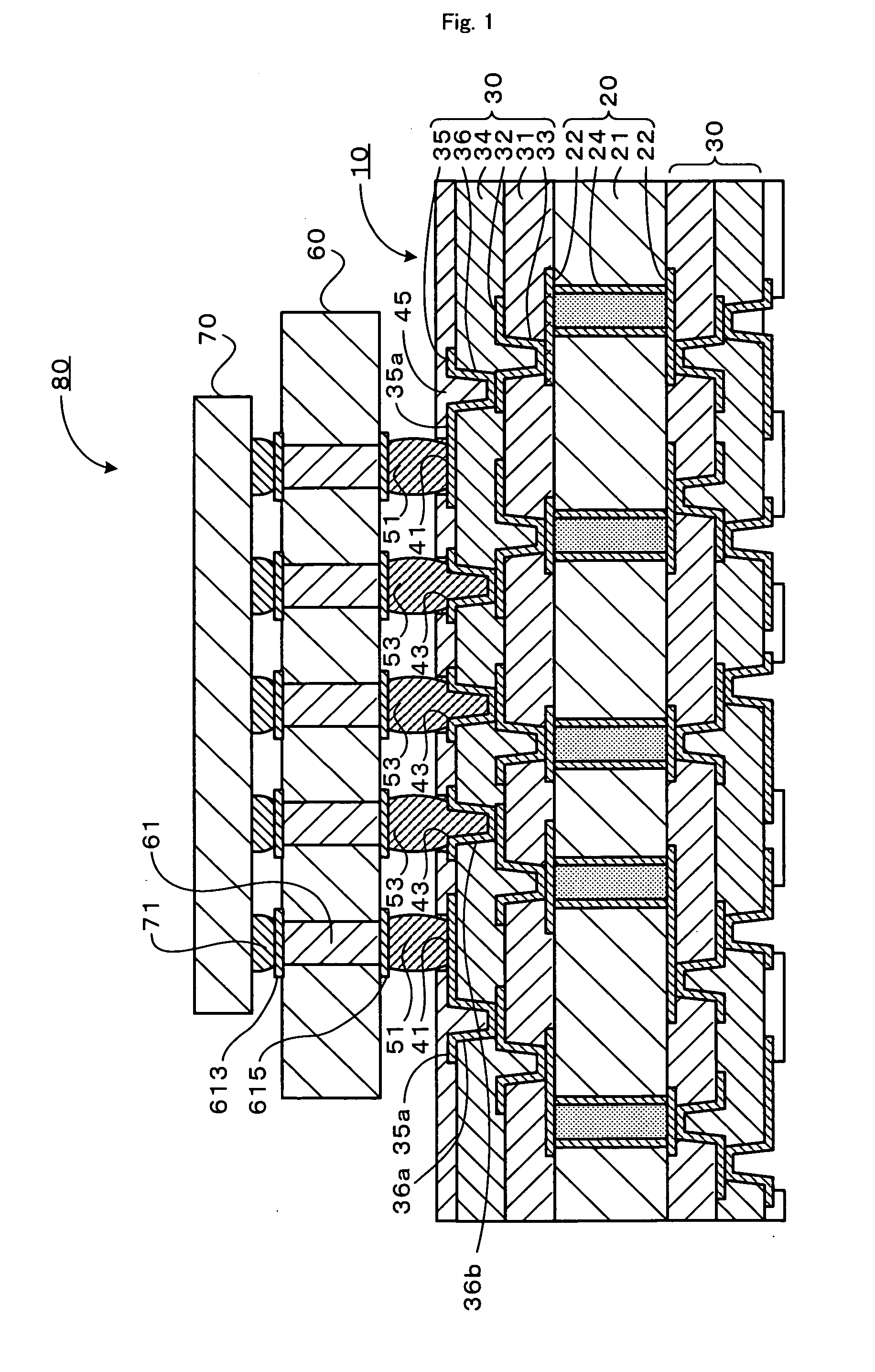
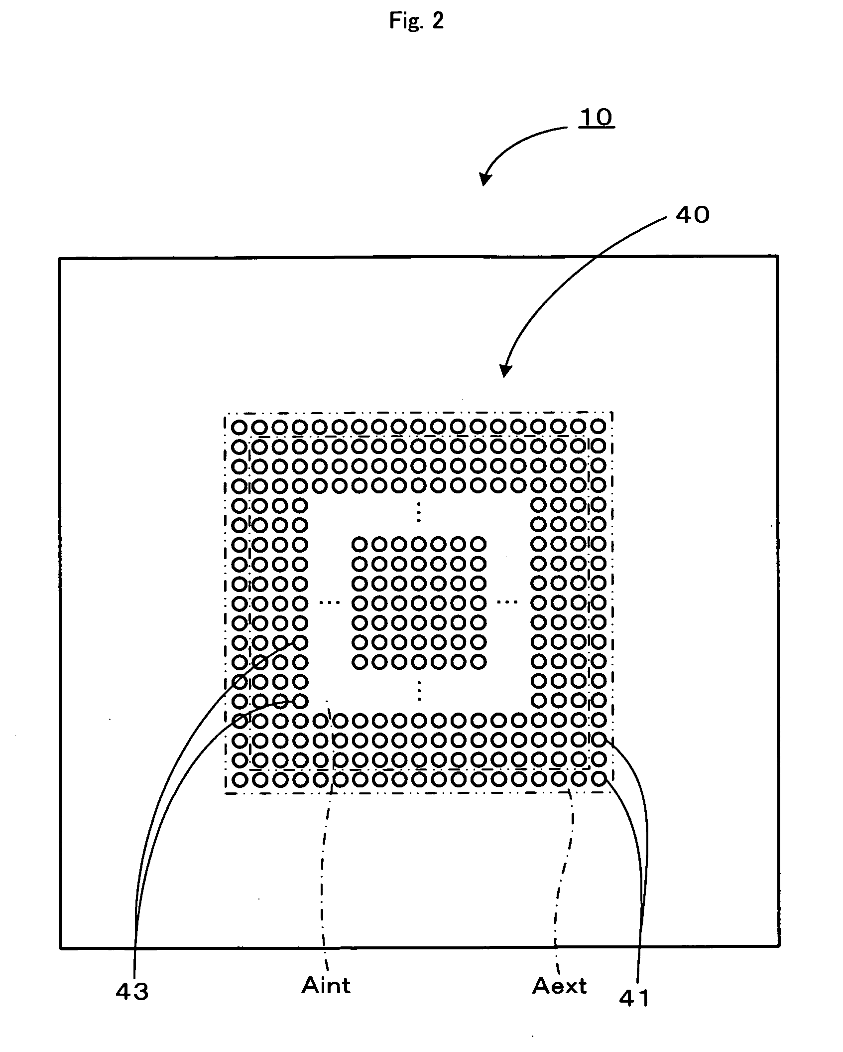
[0072] As shown in the table of FIG. 22, Examples 1 to 8 and Comparative Example 1 of semiconductor mounting boards having external pads and internal pads were prepared in accordance with the manufacturing procedures described above for the embodiment, and with each Example and Comparative Example, an IC chip was mounted via the interposer. In each case, the pad set was formed by arranging 30 by 30 pads of 145 μmf to form a zigzag manner, and the distance between adjacent pads was set to 180 μm (see FIG. 22). In Comparative Example 1, the external pads were arranged as via holes and are connected to the first conductor layers below and the interiors of the holes were not filled with copper plating. With each of these semiconductor mounting boards, the electrical resistance of a specific circuit passing through the IC chip (the electrical resistance across a pair of electrodes, which are exposed on the surface at the side opposite the IC chip mounting surface of the IC chip mounting ...


PUM


Abstract

A semiconductor mounting board 80 is prepared by electrically joining an IC chip 70 via an interposer 60 of high rigidity to external pads 41 and internal pads 43, which are formed on the uppermost surface of a build-up layer 30. When the IC chip 70 generates heat, since pads 41 are positioned away from the center, a large shearing stress is applied to the portions at which pads 41 are joined to the interposer 60 in comparison to the portions at which pads 43 are joined to the interposer 60. Here, pads 41 are formed at substantially flat wiring portions and thus when joined to the interposer 60 by means of solder bumps 51, voids and angled portions, at which stress tends to concentrate, are not formed in the interiors of solder bumps 51. The joining reliability is thus high.

Description

CROSS-REFERENCE TO RELATED APPLICATIONS [0001] This is a continuation application of International Application No. PCT / JP2005 / 003409 filed on Feb. 23, 2005. BACKGROUND OF THE INVENTION [0002] 1. Field of the Invention [0003] This invention concerns a semiconductor mounting board. [0004] 2. Description of the Prior Art [0005] With the progresses in integration circuit (IC) technologies in recent years, the number of input and output terminals of an IC chip is increasing. In order to accommodate for this, a flip-chip method is employed in some cases to mount an IC chip onto a printed wiring board. In this flip-chip method, the input and output terminals are positioned two-dimensionally in a lattice-like, zigzag, or other manner on the main plane of the IC chip, pads are formed at the corresponding positions on a surface of a printed wiring board formed of resin, and these components are joined by solder bumps. Since IC chip is significantly low in thermal expansion coefficient in comp...

Claims


Application Information

Patent Timeline
Patent Type & Authority Applications(United States)
IPC IPC(8): H05K1/09H01L23/12H01L23/498H05K1/11H05K3/46
CPCH01L23/49816H01L23/49833H01L2924/10253H01L23/49838H01L2224/16H01L2924/01046H01L2924/01078H01L2924/01079H01L2924/09701H01L2924/15311H05K1/114H05K3/4602H05K2201/094H05K2201/09472H05K2201/09509H05K2201/10378H05K2201/10734H01L2924/01019H01L2924/00H05K3/46H05K1/14H05K1/03H01L23/12
Inventor OHNO, MASAKITAMAKI, MASANORI
Owner IBIDEN CO LTD
Why Eureka
Try Eureka