

Process for manufacturing a multilayer structure made from semiconducting materials
- Summary
- Abstract
- Description
- Claims
- Application Information
AI Technical Summary
Benefits of technology
Problems solved by technology
Method used
Image

Examples
Embodiment Construction
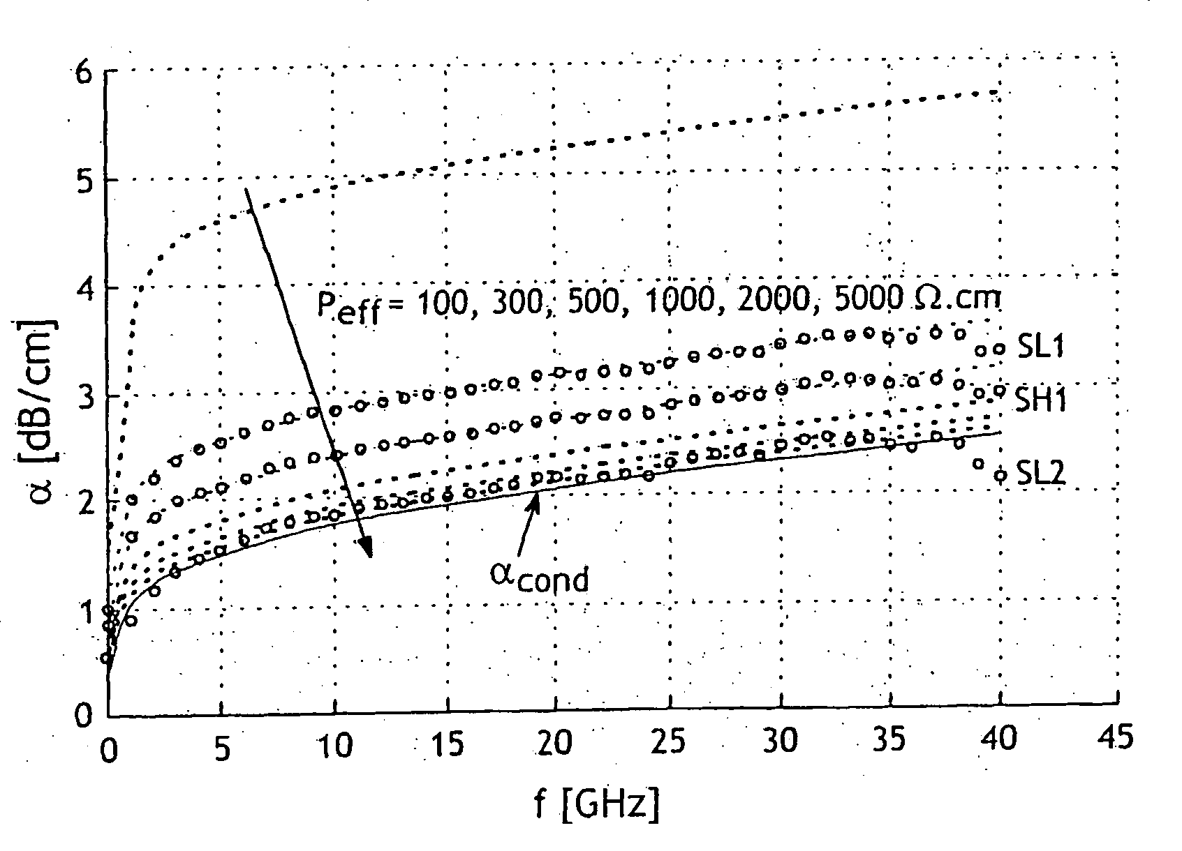
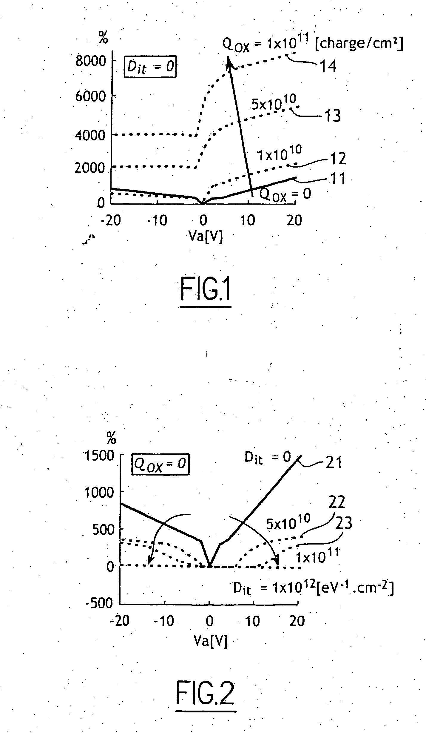
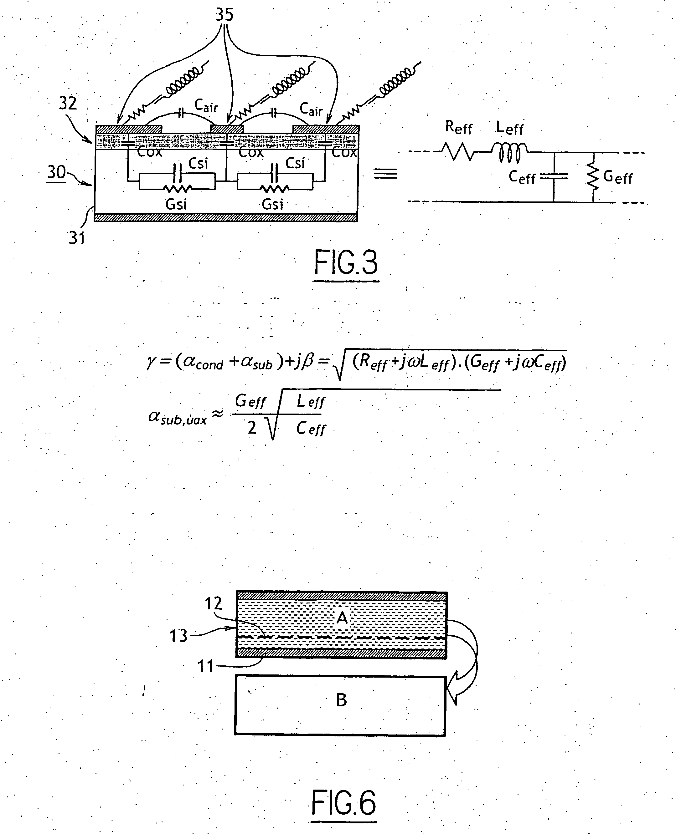
[0028] In order to achieve these purposes, the invention proposes a method of making a multilayer structure made of semiconducting materials and comprising an active layer, a support layer and an electrically insulating layer between the active layer and the support layer, characterized in that the process comprises modification of the density of carrier traps and / or the electrical charge within the electrically insulating layer, in order to minimize electrical losses in the structure support layer.
[0029] Other preferred but non-limitative aspects of such a process are as follows:
[0030] the modification is intended to increase the density of carrier traps at the interface between the structure insulating layer and the structure support layer,
[0031] the modification is designed to reduce the electrical charge within the electrically insulating layer of the structure,
[0032] the active layer is chosen so as to have a much lower resistivity than the support layer,
[0033] the process...
PUM
 Abstract
Description
Claims
Application Information