Electrode for p-type SiC

a technology of silicon carbide and electrode, applied in the direction of semiconductor devices, semiconductor material details, electrical apparatus, etc., can solve the problems of reducing device function and device life, and generally impossible to obtain an ohmic junction between a semiconductor material layer and an electrode without heat treatment, so as to achieve excellent device characteristic, improve surface flatness of electrode, and reduce thermal influence on semiconductor crystal layers

Inactive Publication Date: 2006-08-03
TOYODA GOSEI CO LTD
View PDF4 Cites 3 Cited by
  • Summary
  • Abstract
  • Description
  • Claims
  • Application Information

AI Technical Summary

Benefits of technology

[0013] According to the electrode for p-type SiC configured as described above, the first electrode material exhibiting an eutectic reaction with Al is added. Accordingly, ohmic characteristic can be obtained by a heat-treating step at a low temperature compared with the related art, so that surface flatness of the electrode is improved. In addition, thermal influence on semiconductor crystal layers can be restrained from being caused by the formation of the electrode. Accordingly, the use of the electrode for p-type SiC according to the invention permits production of an SiC device excellent in device characteristic.

Problems solved by technology

In a device using compound semiconductor, it is however generally impossible to obtain an ohmic junction between a semiconductor material layer and an electrode without any heat treatment, that is, Schottky characteristic appears when a metal layer is formed simply.
A problem of reduction in device function and device life caused by deterioration of surface morphology and thermal damage to semiconductor crystal layers has been pointed out.

Method used


Image

  • Electrode for p-type SiC
  • Electrode for p-type SiC

Examples


Embodiment Construction

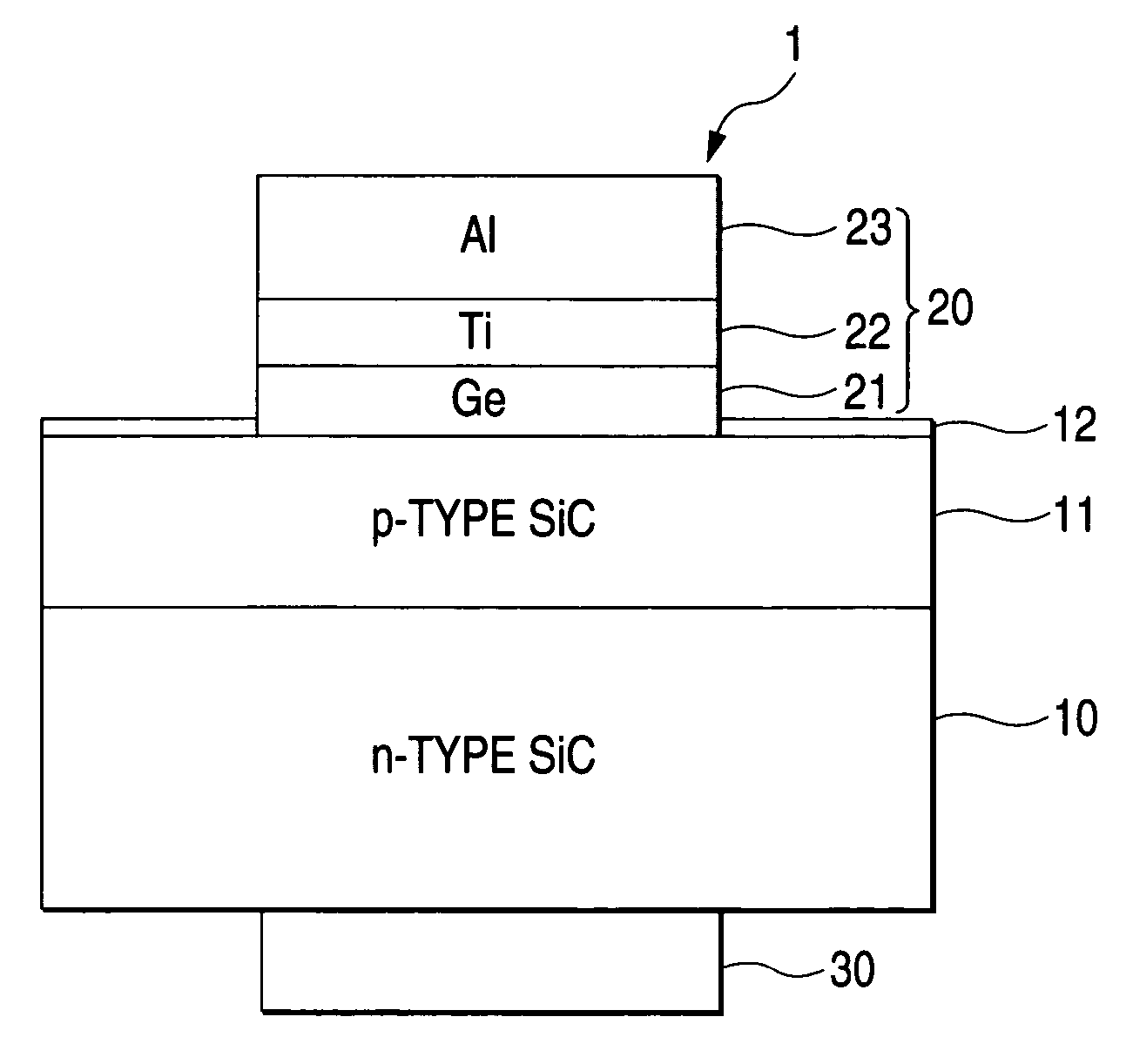
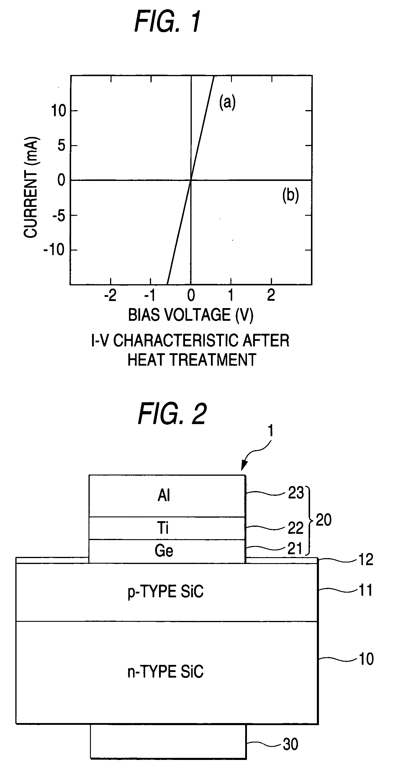
[0017] The term “electrode for p-type SiC” used in the invention means an electrode formed on a p-type SiC semiconductor layer. The configurational type of p-type SiC semiconductor to which the electrode for p-type SiC according to the invention is applied is not particularly limited. Examples of the configurational type of p-type SiC semiconductor include a 4H type used in Embodiment which will be described later, a 6H type, a 15R type, a 21R type, and a 3C type. The kind of the device to which the electrode for p-type SiC according to the invention is applied is not particularly limited either. For example, the electrode for p-type SiC can be applied to various kinds of devices used in a radiofrequency power device, a high-temperature device, an optoelectronic device, etc.

[0018] The first electrode material is not particularly limited if the first electrode material is a material reacting with Si and exhibiting an eutectic reaction with Al at a relatively low temperature. For exa...


PUM

PropertyMeasurementUnit
temperatureaaaaaaaaaa
thickaaaaaaaaaa

Abstract

A p-type electrode containing a first electrode material exhibiting an eutectic reaction at a temperature of 600° C. or lower, and a second electrode material of aluminum (Al).

Description

[0001] The present application is based on Japanese Patent Application No. 2002-314301, which is incorporated herein by reference. BACKGROUND OF THE INVENTION [0002] 1. Field of the Invention [0003] The present invention relates to a silicon carbide (SiC) device. Particularly, it relates to an electrode for p-type SiC, used in an SiC device. [0004] 2. Description of the Related Art [0005] Application of silicon carbide (SiC) to a radiofrequency power device, a high-temperature device and an optoelectronic device has been expected and research toward practical application of silicon carbide (SiC) has advanced. A combination (TiAl) of titanium (Ti) and aluminum (Al) is generally used as a p-electrode for SiC device, that is, an ohmic electrode for p-type SiC (see Patent Document 1 and so on). [0006] [Patent Document 1][0007] Unexamined Japanese Patent Publication No. Hei-5-13812 [0008] Generally, in most cases, a device needs an ohmic electrode. In a device using compound semiconducto...

Claims


Application Information

Patent Timeline
Patent Type & Authority Applications(United States)
IPC IPC(8): H01L31/0312H01L21/28H01L21/04H01L29/24H01L29/45H01L29/861H01L33/34H01L33/40
CPCH01L21/0485H01L29/861H01L29/45H01L29/1608
Inventor SAKAI, TOMOHIROMORIYAMA, MIKIMURAKAMI, MASANORISHIBATA, NAOKI
Owner TOYODA GOSEI CO LTD
Why Eureka
Try Eureka