Systems, masks and methods for printing contact holes and other patterns

Inactive Publication Date: 2006-08-03
PENG DANPING +2
View PDF4 Cites 21 Cited by
  • Summary
  • Abstract
  • Description
  • Claims
  • Application Information

AI Technical Summary

Benefits of technology

[0024] It is understood that each of the above aspects of the invention may be used alone or in combination with one or more other a

Problems solved by technology

However, due to the wave nature of light, as dimensions approach sizes comparable to the wavelength of the exposure light used in the lithography process, the resulting wafer patterns tend to deviate from the corresponding photomask (hereinafter also referred to as “mask”) patterns and degrade due to unwanted distortions and artifacts.
However, such approaches do not consider the full spectrum of possible mask patterns as they set out to generate a suitably pre-distorted pattern, and as a result generate sub-optimal

Method used


Image

  • Systems, masks and methods for printing contact holes and other patterns
  • Systems, masks and methods for printing contact holes and other patterns
  • Systems, masks and methods for printing contact holes and other patterns

Examples


Embodiment Construction

[0044] Reference will now be made in detail to a particular embodiment of the invention, examples of which are illustrated in the accompanying drawings. While the invention will be described in conjunction with the particular embodiments, it will be understood that it is not intended to limit the invention to the described embodiments. To the contrary, it is intended to cover alternatives, modifications, and equivalents as may be included within the spirit and scope of the invention as defined by the appended claims.

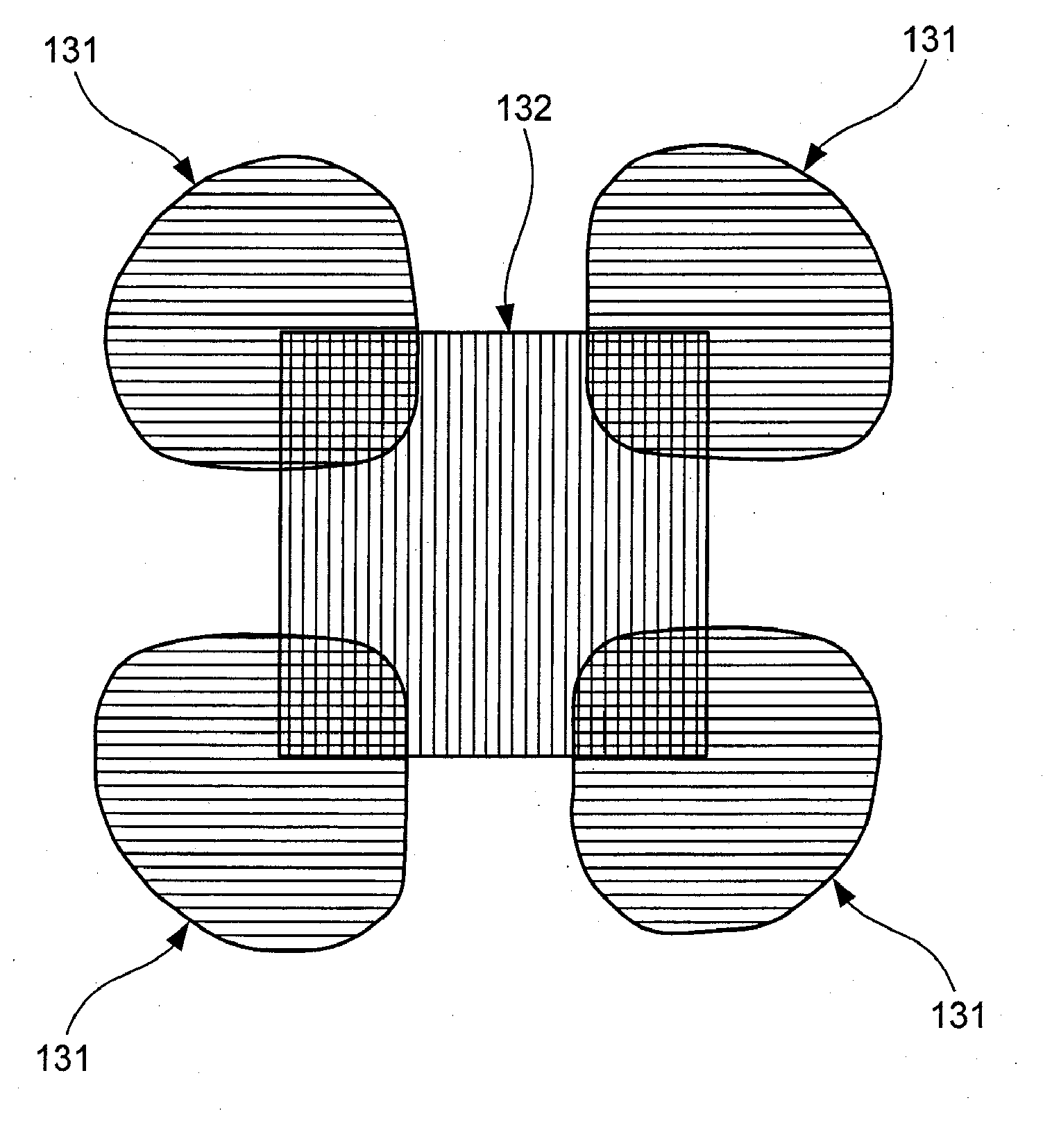
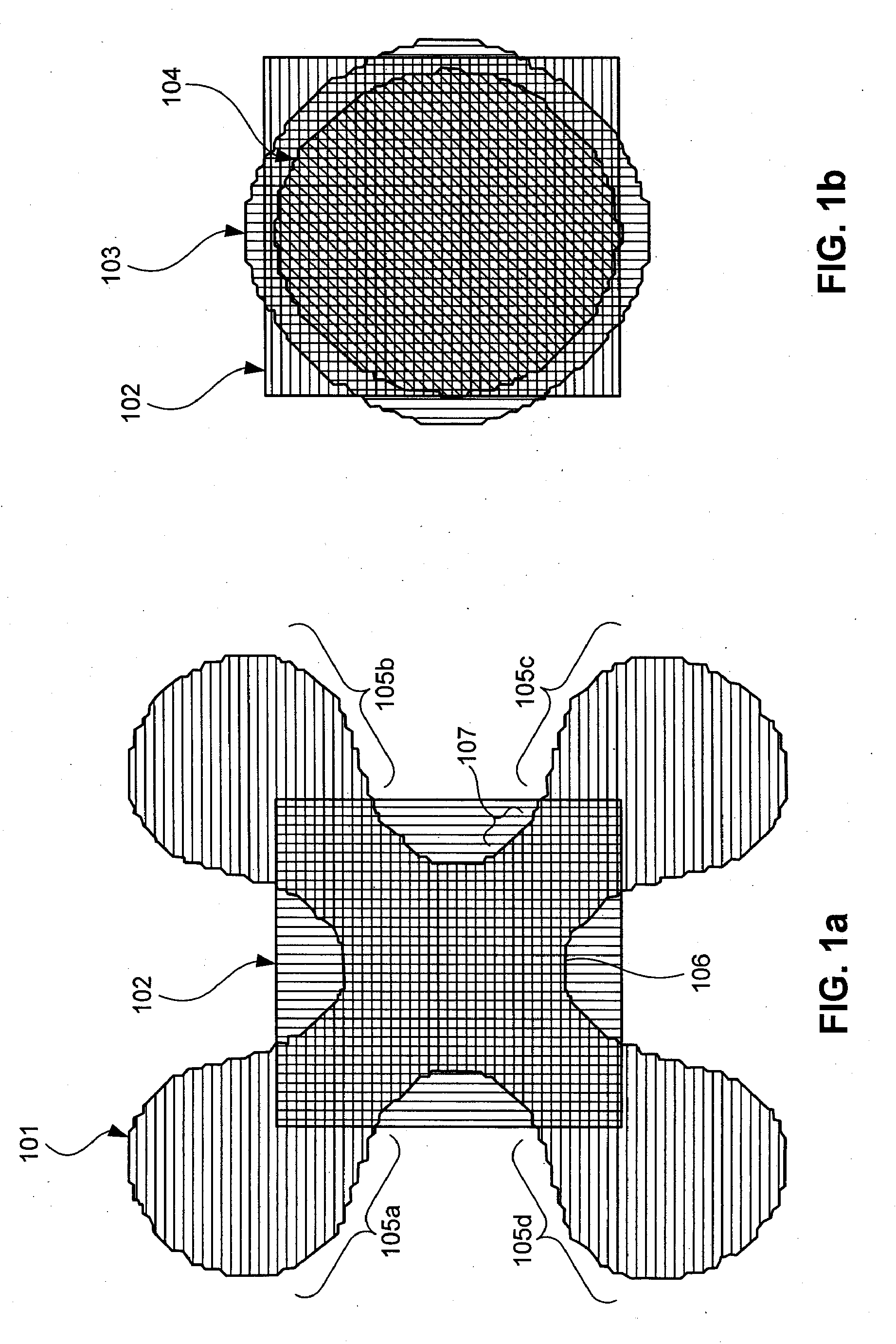
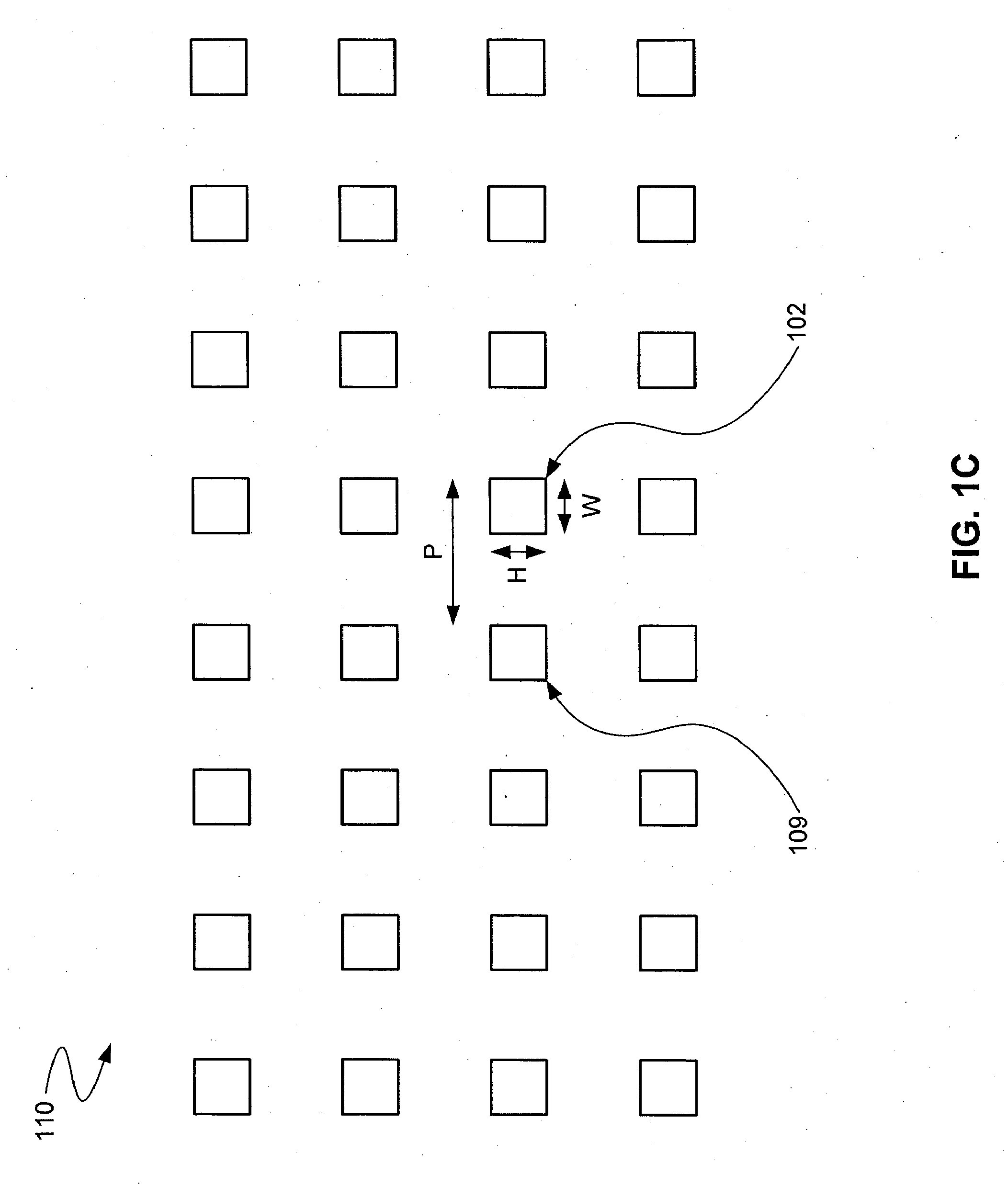
[0045] A contact hole is generally represented in a circuit design as a square, a rectangle, a polygon or other similar shape, to be reproduced as faithfully as possible on a substrate in a lithography process, laser-writer, or direct-write tool. Although it is possible to represent such a contact hole as a corresponding rectangle (or square or polygon), at pattern feature sizes comparable to the wavelength of the exposure light used in the exposure process, exposure li...


PUM


Abstract

Contact hole patterns are disclosed having a plurality of peripheral regions formed around a target area in which a contact hole is to be formed. The peripheral regions visually resemble “lobes” or “leaves” extending outwards towards the periphery of the target area. The lobes may be disjoint or connected to each other. Present methods can be used to prepare masks for printing contact holes on wafers, as well as to prepare design patterns for laser-writers or direct-write lithography in order to print contact holes on masks or directly on wafers. The methods apply to both binary and phase-shift mask designs with varying illuminations.

Description

CROSS REFERENCE [0001] This application claims the benefit of U.S. Provisional Application No. 60 / 723,653, filed Oct. 4, 2005 and U.S. Provisional Application No. 60 / 645,276, filed Jan. 18, 2005, which are incorporated herein by reference in their entirety.FIELD OF INVENTION [0002] The invention pertains in general to semiconductor manufacturing, and in particular to patterns for printing contact holes and other patterns on substrates. BACKGROUND [0003] Lithography processing represents an essential technology for manufacturing integrated circuits (IC) and micro electromechanical devices (MEMS). Lithographic techniques are used to define and write patterns, geometries, features and shapes onto an integrated circuit die or semiconductor wafer. The patterns are generally defined by a set of polygons, contours, lines, boundaries, edges or curves representing or enclosing the boundaries of the regions which constitute the patterns. [0004] Demand for increased density of features on dies...

Claims


Application Information

Patent Timeline
IPC IPC(8): G03C5/00G03F1/00G03F1/36
CPCG03F1/144G03F1/36G03F1/26G03F1/38
Inventor PENG, DANPINGLIU, YONGABRAMS, DANIEL S.
Owner PENG DANPING
Why Eureka
Try Eureka