Micro-oscillating element and method of making the same

a micro-oscillating element and micro-oscillating technology, applied in the direction of fluid pressure measurement, fluid pressure measurement by electric/magnetic elements, instruments, etc., can solve the problems of difficult to achieve a high level of flatness over difficult to achieve a large area of mirror surface flatness, etc., to achieve fast and accurate operation of the movable functional portion, the effect of super-controllability

Active Publication Date: 2006-08-17
FUJITSU LTD
View PDF2 Cites 22 Cited by
  • Summary
  • Abstract
  • Description
  • Claims
  • Application Information

AI Technical Summary

Benefits of technology

[0019] As described above, the present micro-oscillating element has superb controllability over the entire range of oscillating motion of the movable functional porti...

Problems solved by technology

However, according to the surface micromachining technology, the finalized mirror surface is thin and susceptible to warp, and it is difficult to achieve a high level of flatness over a large area of mirror surface.
Likewise, when stopping the mirror support 41 at the rotational displacement of 0°, it is d...

Method used


Image

  • Micro-oscillating element and method of making the same
  • Micro-oscillating element and method of making the same
  • Micro-oscillating element and method of making the same

Examples


first embodiment

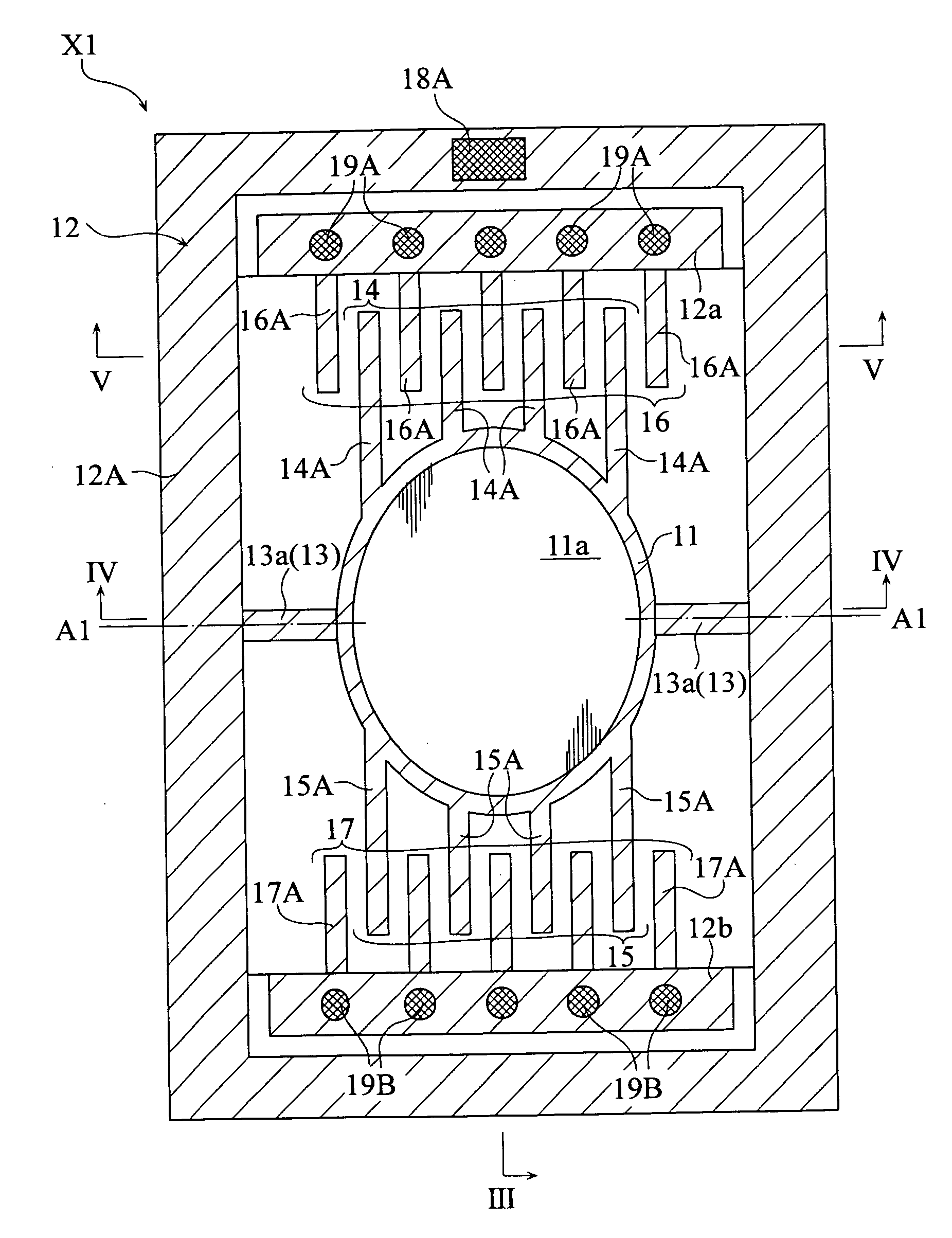
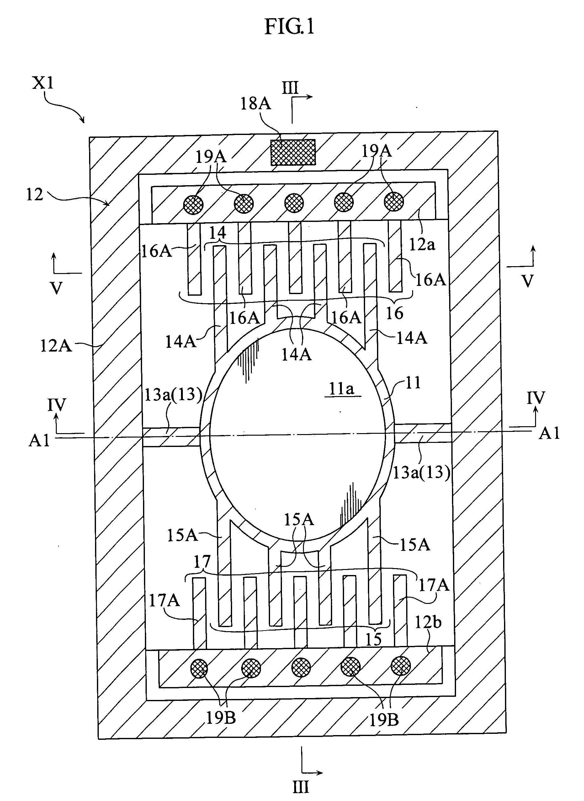
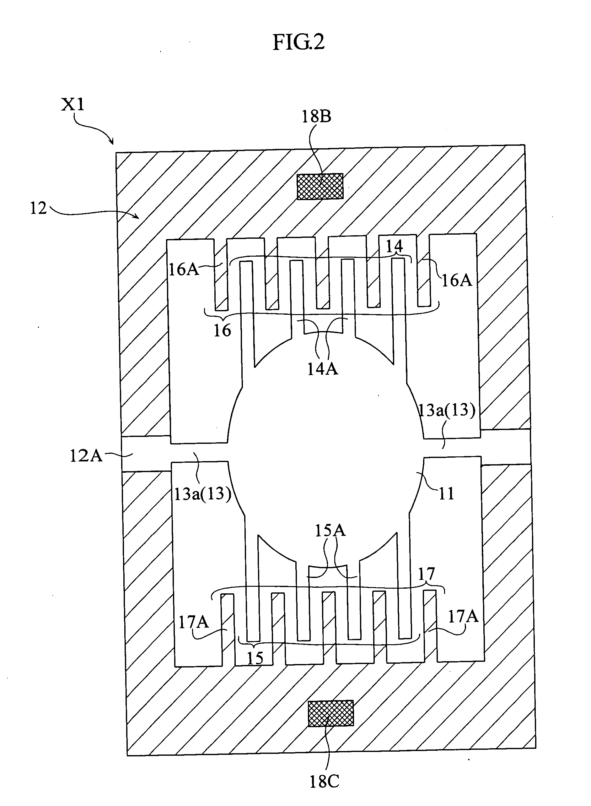
[0063]FIG. 1 through FIG. 5 show a micromirror element X1 according to the present invention. FIG. 1 and FIG. 2 are a front view and a rear view of the micromirror element X1 respectively. FIG. 3 through FIG. 5 are sectional views taken in lines III-III, IV-IV and V-V in FIG. 1 respectively.

[0064] The micromirror element X1 includes a mirror support 11, a frame 12, torsional joint 13 and comb-tooth electrodes 14, 15, 16, 17, and is manufactured by bulk micromachining technology which is a type of MEMS technology, from a material substrate provided by an SOI wafer. The material substrate has a laminate structure composed of a first and a second silicon layers and an insulation layer between the silicon layers. Each silicon layer is doped with impurity, and thereby given a predetermined level of electrical conductivity. Each of the above-mentioned portions in the micromirror element X1 is derived primarily from the first silicon layer and / or the second silicon layer. For the sake of v...

second embodiment

[0095]FIG. 10 through FIG. 14 show a micromirror element X2 according to the present invention. FIG. 10 and FIG. 11 are a front view and a rear view of the micromirror element X2 respectively. FIG. 12 through FIG. 14 are sectional views taken in lines XII-XII, XIII-XIII, and XIV-XIV in FIG. 10 respectively.

[0096] The micromirror element X2 includes a mirror support 21, a frame 22, torsional joint 23 and comb-tooth-electrodes 24, 25, 26, 27, and is manufactured by bulk micromachining technology which is a type of MEMS technology, from a material substrate provided by an SOI wafer. The material substrate has a laminate structure composed of a first and a second silicon layers and an insulation layer between the silicon layers.

[0097] Each silicon layer is doped with impurity, and thereby given a predetermined level of electrical conductivity. Each of the above-mentioned portions in the micromirror element X2 is derived primarily from the first silicon layer and / or the second silicon l...

third embodiment

[0131]FIG. 19 through FIG. 23 show a micromirror element X3 according to the present invention. FIG. 19 and FIG. 20 are a front view and a rear view respectively of the micromirror element X3. FIG. 21 through FIG. 23 are sectional views taken in lines XXI-XXI, XXII-XXII, and XXIII-XXIII in FIG. 19, respectively.

[0132] The micromirror element X3 includes a mirror support 31, a frame 32, a torsional joint 33 and comb-tooth electrodes 34, 35, 36, 37, and is manufactured by bulk micromachining technology such as MEMS technology, from a material substrate provided by a multi-layer SOI wafer. The material substrate has a laminate structure composed of a first through a third silicon layers, a first insulation layer between the first and the second silicon layers, and a second insulation layer between the second and the third silicon layers. Each silicon layer is doped with impurity, and thereby given a predetermined level of electrical conductivity. For the sake of viewing clarity, hatchi...


PUM


Abstract

A micro-oscillating element includes a frame, a movable functional portion, and a torsional joint for joining the frame and the functional portion. The micro-oscillating element also includes first and second comb-tooth electrodes for generation of the driving force for the oscillating motion of the movable functional portion about the torsional joint. The first comb-tooth electrode includes a plurality of first electrode teeth each having a first conductor, an insulator and a second conductor laminated in the direction of the oscillating motion, where the first conductor and the second conductor are electrically connected with each other. The second comb-tooth electrode includes a plurality of second electrode teeth caused not to face the second conductor but to face the first conductor of the first electrode teeth during non-operation. The second electrode teeth are longer than the first conductor in the direction of the oscillating motion.

Description

BACKGROUND OF THE INVENTION [0001] 1. Field of the Invention [0002] The present invention relates to micro-oscillating elements which include a rotationally displaceable part, such as micromirror elements, acceleration sensors, angular speed sensors, vibration elements and so on. [0003] 2. Description of the Related Art [0004] In recent years, efforts have been made for making practical use of elements which have a micro-structure formed by micromachining technology. In the field of optical communications technology for example, micromirror elements which are tiny elements capable of reflecting light are gathering attention. [0005] In the optical communications, optical fibers serve as a medium through which optical signals are passed. When the optical signal passing through a given optical fiber is switched to another optical fiber, so-called optical switching devices are used in general. In order to achieve high quality optical communications, the optical switching device must hav...

Claims


Application Information

Patent Timeline
IPC IPC(8): H01L29/84H01L21/00
CPCB81B2201/04G02B26/0841B81B3/0062B81B2201/033B81B2201/047B81B2203/0109B81B2203/058A47J41/0077A47J39/02A47J41/0083
Inventor KOUMA, NORINAOTSUBOI, OSAMUSONEDA, HIROMITSUUEDA, SATOSHI
Owner FUJITSU LTD
Why Eureka
Try Eureka