Photoelectric conversion layer-stacked solid-state imaging element

a technology of solid-state imaging and photoelectric conversion, which is applied in the field of solid-state imaging elements, can solve the problems of poor production yield of image sensors, the upper limit of the amount of photocharge that can be stacked in one fine light-receiving portion, and the slow progress of ccd-type image sensors and cmos-type images, etc., and achieves high-quality color images.

Inactive Publication Date: 2006-08-17
FUJIFILM CORP
View PDF4 Cites 92 Cited by
  • Summary
  • Abstract
  • Description
  • Claims
  • Application Information

AI Technical Summary

Benefits of technology

[0022] An aim of the invention is to provide a photoelectric conversion layer-stacked solid-state imaging element which can sufficiently separate signal charge by pixels and avoid color mixing among pixels to take a high quality color image.

Problems solved by technology

However, the technical progress of CCD type image sensors and CMOS type images has been almost limited.
Therefore, these types of image sensors face a problem of poor yield in production.
Further, the upper limit of the amount of photocharge that can be stacked in one fine light-receiving portion is as low as about 3,000 electrons, with which 256 gradations can be difficultly expressed completely.
Therefore, it has been difficult to expect CCD type or CMOS type image sensor that outperforms the related art products from the standpoint of image quality or sensitivity.
Further, problem of color mixing among pixels cannot be neglected.

Method used


Image

  • Photoelectric conversion layer-stacked solid-state imaging element
  • Photoelectric conversion layer-stacked solid-state imaging element
  • Photoelectric conversion layer-stacked solid-state imaging element

Examples


first embodiment

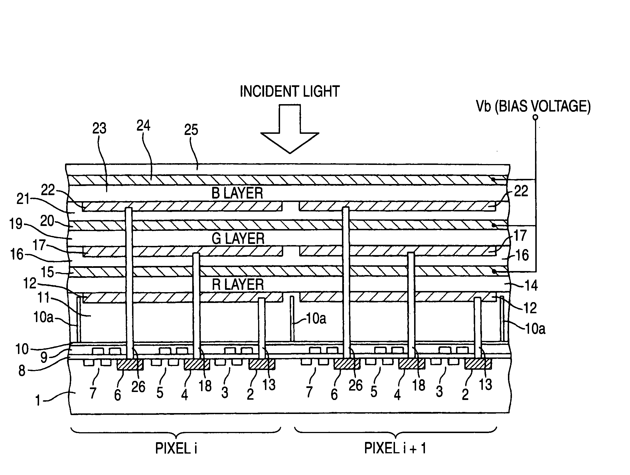
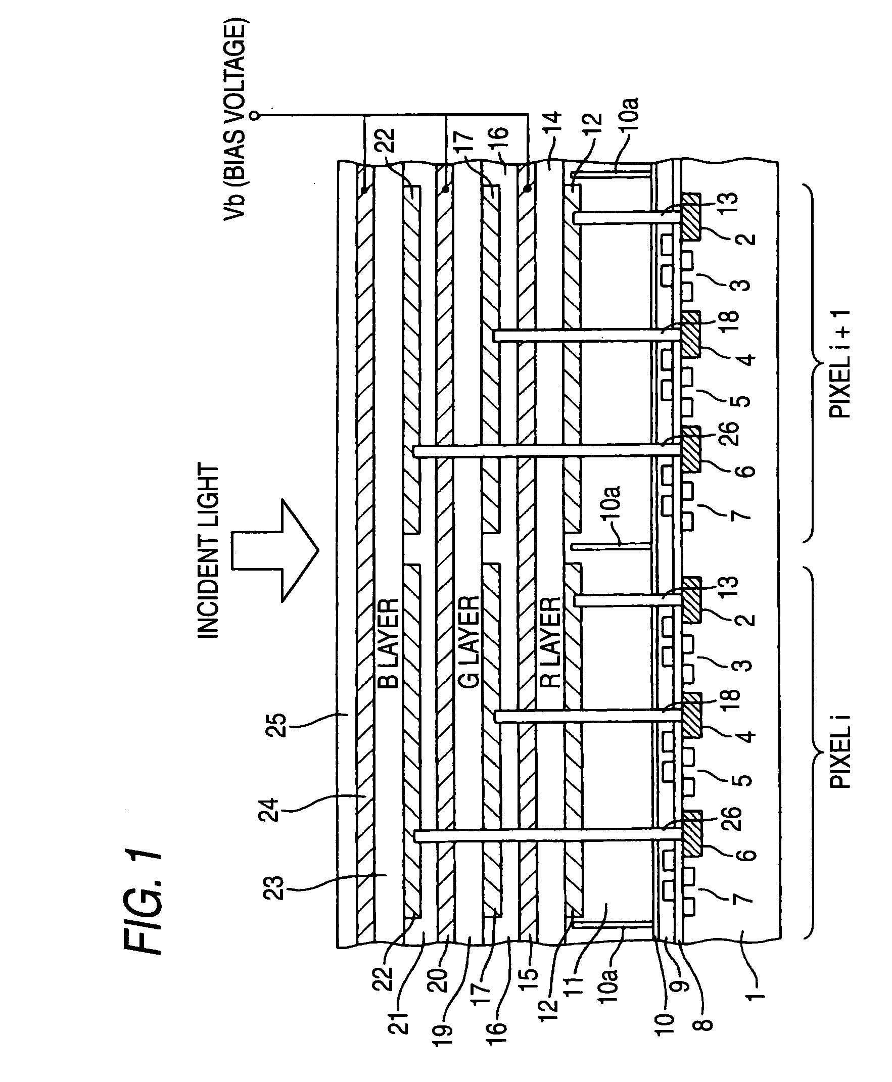
[0035]FIG. 1 is a diagrammatic sectional view of a two pixel portion of a photoelectric conversion layer-stacked solid-state imaging element according to a first embodiment of implementation of the invention. Since the basic configuration of the present embodiment is the same as that of the related art photoelectric conversion layer-stacked solid-state imaging element explained in FIG. 5, like numerals are used where the members are the same as those of the related art photoelectric conversion layer-stacked solid-state imaging element. Where the members are the same as those of the related art photoelectric conversion layer-stacked solid-state imaging element, no description is made.

[0036] In the photoelectric conversion layer-stacked solid-state imaging element according to the present embodiment, a shielding wall 10a made of the same material as that of a light shielding layer 10 is provided erected on the light shielding layer 10 at the pixel border portion in an insulating laye...

second embodiment

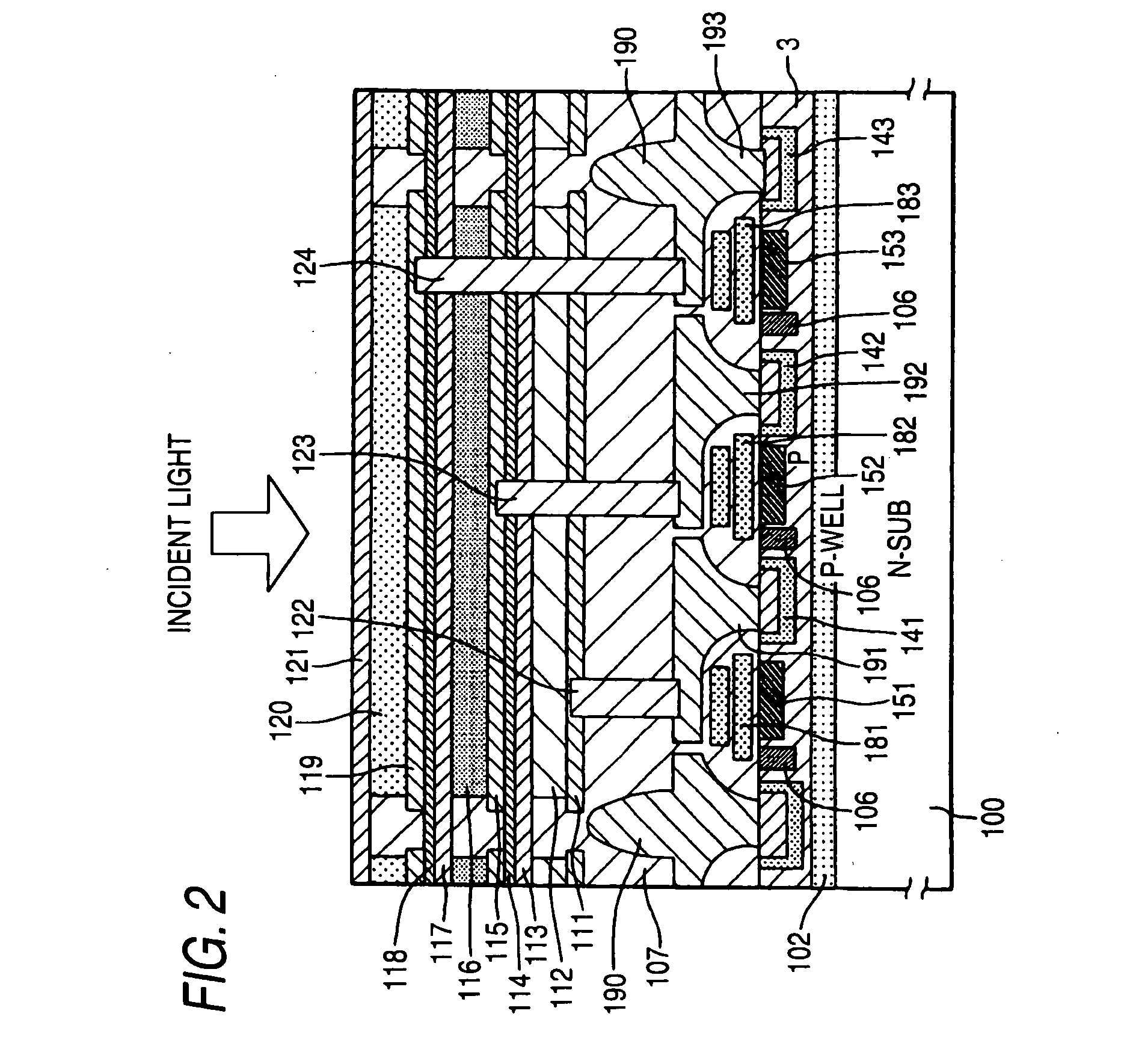
[0037]FIG. 2 is a diagrammatic sectional view of a one pixel portion of a photoelectric conversion layer-stacked solid-state imaging element according to a second embodiment of implementation of the invention. On the surface portion of a semiconductor substrate 100 is formed a signal reading circuit. The signal reading circuit may be formed by an MOS transistor circuit as in FIG. 1. In the present embodiment, however, the signal reading circuit is formed by a charge transmission channel as in the related art CCD type image sensor.

[0038] In the photoelectric conversion layer-stacked solid-state imaging element shown in FIG. 2, a P-well layer 102 is formed on the surface portion of an n-type semiconductor substrate 100. In a P-region 103 on the surface portion of the P-well layer 102 are formed a diode portion 141 which is a first color charge accumulating region, a diode portion 142 which is a second color charge accumulating region and a diode portion 143 which is a third color cha...

third embodiment

[0053]FIG. 3 is a diagram illustrating the configuration of the light shielding layer (lower electrode) of a photoelectric conversion layer-stacked solid-state imaging element according to a third embodiment of implementation of the invention. In the first and second embodiments, the shape of the portion of the light shielding layer interposed between the shielding walls (convex portion) 10a and 190 provided at the pixel border portion is flat. However, the photoelectric conversion layer-stacked solid-state imaging element according to the present embodiment is arranged such that light reflected by the light shielding layer under the original pixel goes toward the original pixel rather than the adjacent pixels.

[0054] In some detail, in the photoelectric conversion layer-stacked solid-state imaging element according to the present embodiment, the surface of the lower electrode interposed between the shielding walls 190 is concave such that the surface level is low at the central por...


PUM


Abstract

A photoelectric conversion layer-stacked solid-state imaging element comprises: a semiconductor substrate having a signal reading circuit formed thereon; at least one layer of photoelectric conversion layer each of which is provided interposed between a common electrode layer and a plurality of pixel electrode layers corresponding to pixels, said at least one layer of photoelectric conversion layer being stacked above the semiconductor substrate via a light shielding layer; and inhibiting structures each of which inhibits a reflected light produced by reflection of incident light on the light shielding layer, the incident light having passed through said at least one layer of photoelectric conversion layer and entered into a pixel, from entering in direction toward adjacent pixels.

Description

BACKGROUND OF THE INVENTION [0001] 1. Field of the Invention [0002] The present invention relates to a solid-state imaging element comprising a plurality of photoelectric conversion layers stacked on a semiconductor substrate having a signal reading circuit formed thereon and particularly to a photoelectric conversion layer-stacked solid-state imaging element comprising a light shielding layer provided interposed between the lowermost photoelectric conversion layer and the semiconductor substrate. [0003] 2. Description of the Related Art [0004] A prototype example of photoelectric conversion layer-stacked solid-state imaging element is one disclosed in JP-A-58-103165. This solid-state imaging element comprises three light-sensitive layers stacked on a semiconductor substrate. In this arrangement, Red (R), green (G) and blue (B) electrical signals detected in the respective light-sensitive layer are read out by MOs circuit formed on the semiconductor substrate. [0005] The solid-state...

Claims


Application Information

Patent Timeline
Patent Type & Authority Applications(United States)
IPC IPC(8): H04N5/335H01L27/14H01L27/146H04N5/369H04N9/07
CPCH01L27/14609H01L27/14623H01L27/14625H01L27/14647H01L27/14692H04N2209/047
Inventor MIYASHITA, TAKESHIMISAWA, TAKESHI
Owner FUJIFILM CORP
Why Eureka
Try Eureka