Method of manufacturing floating structure

a floating structure and manufacturing method technology, applied in the manufacture of microstructure devices, microstructure technology, electric devices, etc., can solve problems such as design value errors, and achieve the effect of increasing the yield of devices

Inactive Publication Date: 2006-08-17
SAMSUNG ELECTRONICS CO LTD
View PDF2 Cites 38 Cited by
  • Summary
  • Abstract
  • Description
  • Claims
  • Application Information

AI Technical Summary

Benefits of technology

[0013] The present invention has been made to solve the above-mentioned problems of the prior art, and an object

Problems solved by technology

Such notches 32 change the physical properties such as mass and spring consta

Method used


Image

  • Method of manufacturing floating structure
  • Method of manufacturing floating structure
  • Method of manufacturing floating structure

Examples


Embodiment Construction

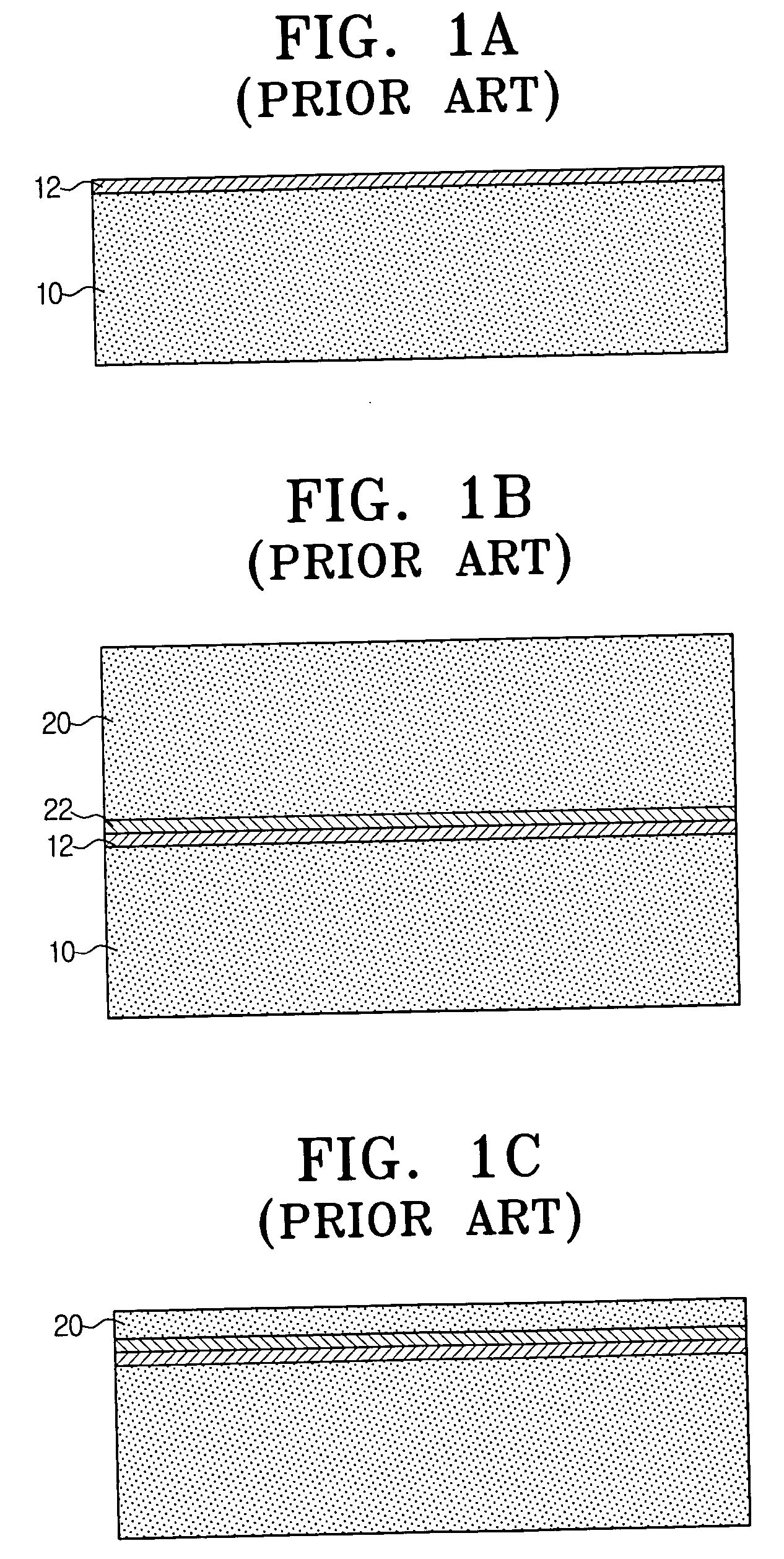
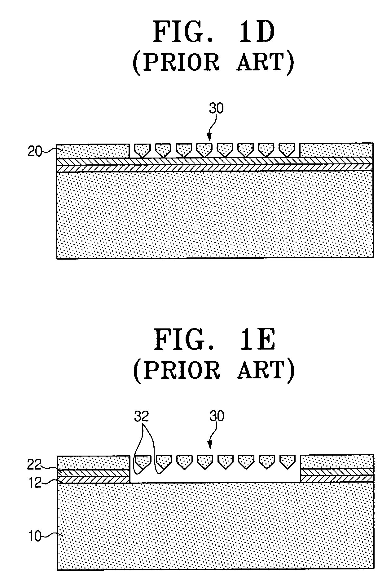
[0023] Hereinbelow, embodiments of the present invention are described in detail with reference to the accompanying drawings. However, the present invention should not be construed as being limited thereto.

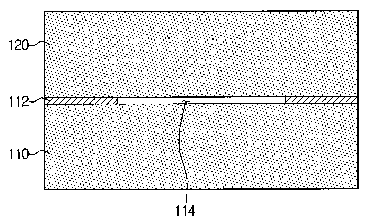
[0024] Referring to FIG. 2E, a floating structure 130 according to an embodiment of the present invention has a floating structure 130 formed by etching a second substrate 120, so that the floating structure 130 floats at a predetermined distance above the top side of a first substrate 110. Although not shown in the drawing, the floating structure 130 is partially supported by the first substrate 110, the second substrate 120 and / or an insulation film 112. For example, the floating structure 130 may comprise a projection portion which projects over predetermined area 114. The insulation film 112 is interposed between the first substrate 110 and the second substrate 120 to electrically isolate the first substrate 110 and the second substrate 120. The floating structure 130 configu...


PUM

PropertyMeasurementUnit
Thicknessaaaaaaaaaa
Areaaaaaaaaaaa

Abstract

A method of manufacturing a floating structure capable of providing increased device yield. The method includes: a) forming an insulation film, a predetermined area of which is removed, between a first substrate and a second substrate; and b) forming a floating structure in the removed predetermined area.

Description

CROSS-REFERENCE TO RELATED APPLICATIONS [0001] This application claims the benefit of Korean Patent Application No. 2005-11836 filed on Feb. 14, 2005 in the Korean Intellectual Property Office, the disclosure of which is incorporated herein by reference. BACKGROUND OF THE INVENTION [0002] 1. Field of the Invention [0003] The present invention relates to a method of manufacturing a micro floating structure capable of providing improved device yield. [0004] 2. Description of the Related Art [0005] A micro floating structure as mentioned above is used as an inertia weight, a spring or the like in a sensor such as an accelerometer or gyroscope. A conventional method of manufacturing such a micro floating structure is illustrated in FIGS. 1A to 1E. [0006] Referring to FIGS. 1A and 1B, according to the conventional method, first and second oxide films 12, 22 are formed on one surface of each of first and second substrates 10, 20, respectively, and then the first and second substrates 10, ...

Claims


Application Information

Patent Timeline
IPC IPC(8): H01L21/302
CPCB81C1/0015B81C2201/019H01L21/3065H10K99/00
Inventor KANG, SEOK-JIN
Owner SAMSUNG ELECTRONICS CO LTD
Why Eureka
Try Eureka