Nitride semiconductor free-standing substrate

a technology of nitride and semiconductor, applied in the direction of polycrystalline material growth, crystal growth process, chemically reactive gas, etc., can solve the problems of difficult to obtain a high-quality growth layer, substrate must have a considerable number of crystal defects, and the device characteristics cannot be improved. , to achieve the effect of reducing the variation of emission wavelength, reducing the emission output, and reducing the emission of crystal defects

Active Publication Date: 2007-12-20
SUMITOMO CHEM CO LTD
View PDF6 Cites 25 Cited by
  • Summary
  • Abstract
  • Description
  • Claims
  • Application Information

AI Technical Summary

Benefits of technology

[0024]The nitride semiconductor free-standing substrate of the invention can provide a light emitting device structure to provide a reduced variation in emission wavelength, emission output, lifetime etc. of the device, and can provide many light emitting devices with desired properties according to the designed values.
[0025]Thus, in producing a nitride semiconductor light emitting device by using the nitride semiconductor free-standing substrate, the yield of the device can be drastically increased.

Problems solved by technology

However, it was difficult to obtain a high quality growth layer since no underlying substrate is found which lattice-matches to the nitride-based semiconductor layer.
The crystal defect is an impediment to the improvement of the device characteristics.
However, even when conducting the growth method using the low temperature deposition buffer layer, the resultant substrate must have a considerable number of the crystal defects such as a penetrating dislocation and a void.
Therefore, this method is insufficient for producing a presently-desired high-performance device.
Thus, it is difficult to grow thereon an epitaxial layer for a device.
However, according to further researches of the inventor, it is found that, when plural devices are fabricated by growing a light emitting device structure on the GaN free-standing substrate and being mounted, a large variation in emission wavelength are recognized among the devices, and some of the devices have a very low emission output and lifetime.

Method used


Image

  • Nitride semiconductor free-standing substrate
  • Nitride semiconductor free-standing substrate
  • Nitride semiconductor free-standing substrate

Examples


example 1

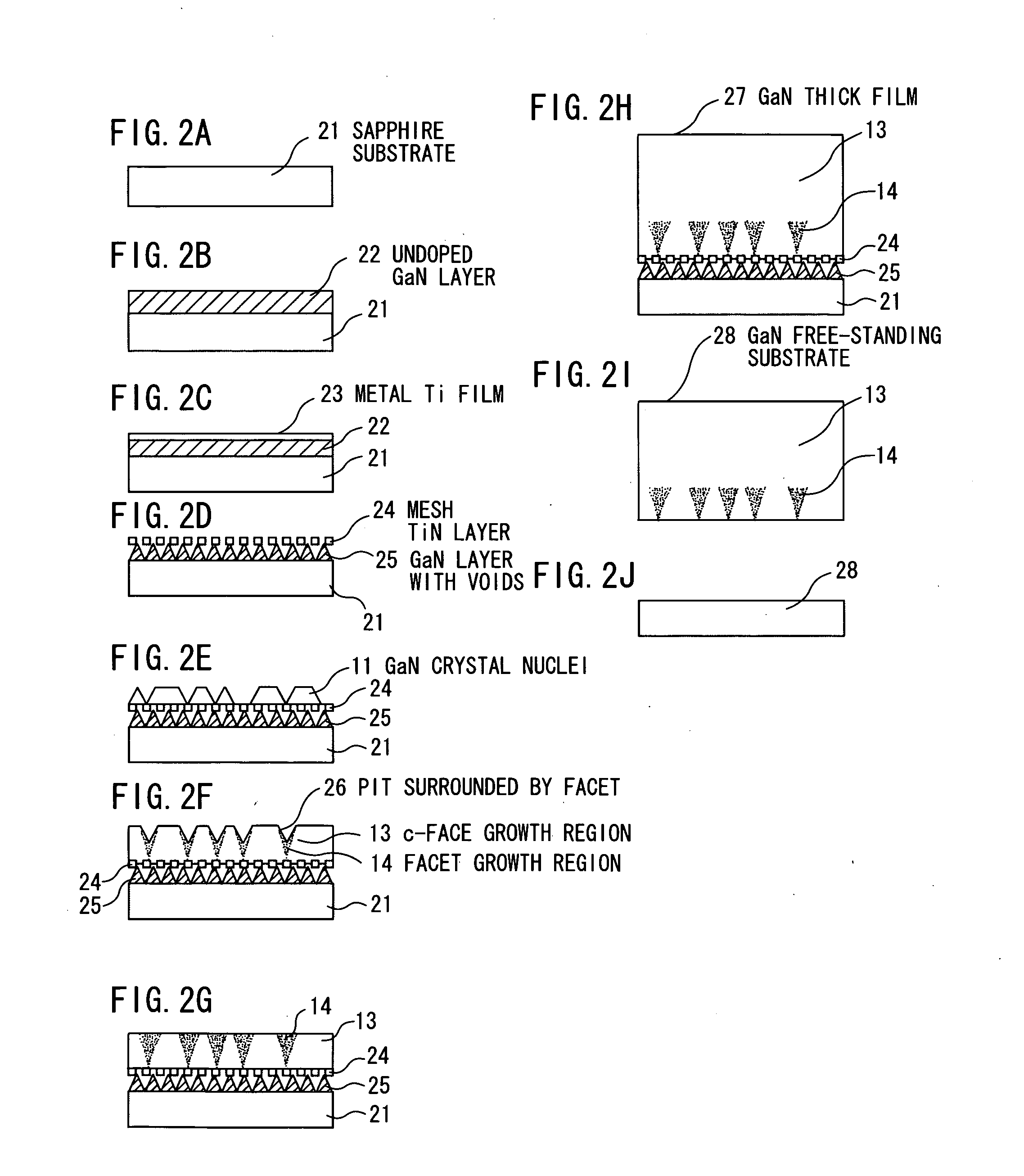
[0048]A GaN epitaxial layer is grown on a sapphire substrate by VAS (void-assisted separation) method and then a GaN free-standing substrate is formed by removing the sapphire substrate and was evaluated. The details of the VAS method are described in JP-A-1999-251253. In brief, the VAS method is a method that crystal growth is conducted sandwiching a titanium nitride (TiN) layer with a mesh structure between the sapphire substrate and a GaN growth layer.

[0049]A method of making a GaN free-standing substrate of Example 1 will be explained below with reference to FIGS. 2A to 2J.

[0050]At first, a single crystal c-face sapphire substrate 21 of 2 inches diameter is provided (FIG. 2A) and, on the sapphire substrate 21, an undoped GaN layer 22 is grown 300 nm in thickness using trimethylgallium (TMG) and NH3 (FIG. 2B) by MOVPE method. Then, a metal Ti film 23 is deposited 20 nm in thickness on the GaN layer 22 (FIG. 2C), and it is placed in an electric furnace and heated at 1050° C. for 2...

example 2

[0056]A void-formed substrate is placed in the HVPE furnace and the GaN substrate is grown thereon using as precursors NH3 and GaCl and as a carrier gas a mixing gas of 5% H2 and 95% N2. The growth conditions used are atmospheric pressure and substrate temperature of 1040° C. Partial pressures of GaCl and NH3 in the supply gas are set 8×10⁻³ atm and 5.6×10⁻² atm, respectively, at the beginning of growth, and its V / III ratio is set 7. In the growth process of the GaN crystal, doping material gas of SiH2Cl2 is supplied to the substrate region to dope Si.

[0057]When the whole thickness reaches 100 μm, by changing the growth conditions into conditions (i.e., substrate temperature of 1080° C. and a V / III ratio of 2) to advance the flattening, the flattening is completed before reaching about 250 μm in the whole thickness. After the completion of the flattening, the V / III ratio is back to 7 and the GaN thick film is grown until having 400 μm in the whole thickness.

[0058]In the cooling proc...

example 3

[0060]A void-formed substrate is placed in the HVPE furnace and the GaN substrate is grown thereon using as precursors NH3 and GaCl and as a carrier gas a mixing gas of 5% H2 and 95% N2. The growth conditions used are atmospheric pressure and substrate temperature of 1040° C. Partial pressures of GaCl and NH3 in the supply gas are set 8×10⁻³ atm and 5.6'10−2 atm, respectively, at the beginning of growth, and its V / III ratio is set 7. In the growth process of the GaN crystal, doping material gas of SiH2Cl2is supplied to the substrate region to dope Si.

[0061]When the whole thickness reaches 200 μm, by changing the growth conditions into conditions (i.e., substrate temperature of 1080° C. and a V / III ratio of 2) to advance the flattening, the flattening is completed before reaching about 350 μin the whole thickness. After the completion of the flattening, the V / III ratio is back to 7 and the GaN thick film is grown until having 400 μm in the whole thickness.

[0062]In the cooling process...


PUM

PropertyMeasurementUnit
thicknessaaaaaaaaaa
thicknessaaaaaaaaaa
thicknessaaaaaaaaaa

Abstract

A nitride semiconductor free-standing substrate formed of a free-standing nitride-based compound semiconductor crystal that has a variation in lattice constant of ±12 ppm or less.

Description

[0001]The present application is based on Japanese patent application No. 2006-164573, the entire contents of which are incorporated herein by reference.BACKGROUND OF THE INVENTION[0002]1. Field of the Invention[0003]This invention relates to a nitride semiconductor free-standing substrate comprising a nitride-based compound semiconductor crystal and a light emitting device using the substrate. In particular, this invention relates to a nitride semiconductor free-standing substrate that can provide a light emitting device, which is fabricated by using the substrate, with a small variation in emission wavelength, emission output, device lifetime etc., and that can provide the light emitting device with an enhanced yield, and relates to the light emitting device using the substrate.[0004]2. Description of the Related Art[0005]Nitride semiconductor materials have a sufficiently wide bandgap and are of direct transition type in inter-band transition. Therefore, they are a great deal res...

Claims


Application Information

Patent Timeline
Patent Type & Authority Applications(United States)
IPC IPC(8): H01L31/00H01L33/06H01L33/32H01L33/42
CPCC30B25/18C30B29/403H01L21/0242H01L21/02491H01L33/0075H01L21/0262H01L21/02639H01L21/02647H01L21/0254
Inventor YOSHIDA, TAKEHIRO
Owner SUMITOMO CHEM CO LTD
Why Eureka
Try Eureka