Semiconductor device and method for fabricating same

a technology of semiconductor devices and semiconductor oxide films, which is applied in the direction of semiconductor devices, semiconductor/solid-state device details, electrical equipment, etc., can solve the problems of increasing leak current, affecting the yield of devices, and affecting the quality of gate oxide films, so as to improve the yield of devices and improve the device characteristics

Inactive Publication Date: 2009-04-23
SHARP KK
View PDF6 Cites 20 Cited by
  • Summary
  • Abstract
  • Description
  • Claims
  • Application Information

AI Technical Summary

Benefits of technology

[0028]According to the present invention, since the gettering site is provided immediately under the device forming region, in any devices such as a device of which thin device chips is required and a device of which extreme thinness of device chips for an IC card and the like is required, degradation of device characteristics and reliability caused by contamination of metal impurities can be inhibited, which leads to stability and improvement of the yield of devices.

Problems solved by technology

Factors of degradation of the characteristics and reliability of the devices include an increase in leak current caused by occurrence of crystal defect and degradation of the film quality of the gate oxide film, which are based on contamination of metal impurities.
In the EG method, if the IC chip is as extremely thin as equal to or less than 100 μm, it is difficult in terms of strength to introduce lattice distortion or defect on the back surface.
If the back surface of the silicon semiconductor substrate is subjected to mechanical grinding, the back surface becomes rough, which leads to introduction of defect to generate the EG effect of gettering of metal impurities.
However, if the silicon semiconductor substrate becomes extremely thin, the bending strength of the substrate becomes weak, and thus if the back surface is rough, the substrate becomes easy to crack.
However, mirror processing eliminates the EG effect of gettering of metal impurities, which leads to, due to contamination of metal impurities, degradation of device characteristics and reliability.

Method used


Image

  • Semiconductor device and method for fabricating same
  • Semiconductor device and method for fabricating same
  • Semiconductor device and method for fabricating same

Examples


example 1

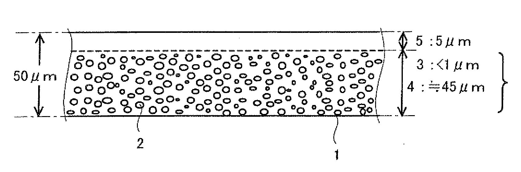
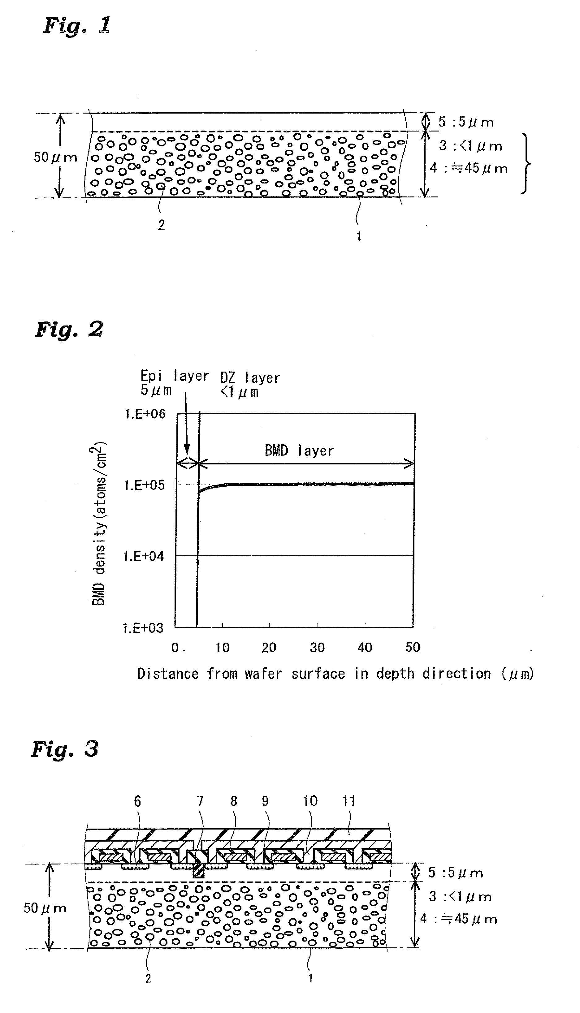
[0068]Example 1 relates to a method for forming BMD of an oxygen precipitates to serve as a gettering site for metal impurities immediately under a device forming region.

[0069]Referring to FIG. 1, a silicon semiconductor substrate 1 is prepared in which a BMD 2 is formed up to the substrate surface (so that the thickness of a DZ layer is equal to or less than 1 μm) by adjusting the speed of pulling up an ingot Si crystal to serve as the semiconductor substrate and the temperature distribution of the pulling up furnace. On the silicon semiconductor substrate 1, a 5-μm thick epitaxial Si layer 5 to serve as a device forming region is formed by heat treatment of 1200° C. In this case, it is preferable that prior to formation of the epitaxial Si layer 5, the silicon semiconductor substrate 1 is subjected to heat treatment to shrink the BMD 2, thereby preventing crystal dislocation that occurs during growth of the epitaxial Si layer 5. This makes the number of the BMD 2 1E+05 / cm2 formed ...

example 2

[0074]Example 2 relates to a method for forming a Si crystal distortion to serve as a gettering site for metal impurities immediately under a device forming region.

example 2-1

[0075]Referring to FIG. 5(A), an ion plantation of the inactive element Ar is carried out at a high energy of 5 MeV in a dose of approximately 5E+15 / cm2 to the silicon semiconductor substrate 1, thereby forming a Si crystal distortion 12 at the depth of approximately 5 μm from the substrate surface and immediately under the device forming region. In order to promote recrystallization of the Si that has been turned into amorphousness by the ion plantation, heat treatment is carried out at 900° C. for approximately 30 minutes. This enables it to form the Si crystal distortion 12 to serve as the gettering site for metal impurities immediately under the device forming region.

[0076]FIG. 5(B) shows the flow of example 2-1.


PUM

PropertyMeasurementUnit
thicknessaaaaaaaaaa
thicknessaaaaaaaaaa
thicknessaaaaaaaaaa

Abstract

A semiconductor device has an IC chip with a thickness of equal to or less than 100 μm and includes a semiconductor substrate. A device forming region is within the depth of approximately equal to or less than 5 μm from a surface of the semiconductor substrate, and a total thickness of the semiconductor substrate is from 5 μm to 100 μm. A BMD layer for carrying out gettering of metal impurities is provided immediately under the device forming region. Since a gettering site is provided immediately under the device forming region, in a device or the like of which extreme thinness is required, degradation of device characteristics and reliability due to contamination of metal impurities can be prevented, and stabilize and improve the device yield. The present invention inhibits degradation of device characteristics and reliability caused by contamination of metal impurities, in a device of which lamination of device chips is required or in a device of which extreme chip thinness for an IC card and the like is required, in an attempt to cope with an enlarged capacity of the device.

Description

TECHNICAL FIELD[0001]The present invention generally relates to semiconductor devices, and more particularly to a semiconductor device improved to inhibit degradation of device characteristics and decrease in reliability which are caused by contamination of metal impurities, in a device wherein thin device chips and extreme thin chip for an IC card are required, in order to correspond to an enlarged capacity of the device.BACKGROUND ART[0002]In the fabrication of semiconductor devices, in order to stabilize and improve the yield of the devices, it is required to inhibit degradation of the characteristics and reliability of the devices. Factors of degradation of the characteristics and reliability of the devices include an increase in leak current caused by occurrence of crystal defect and degradation of the film quality of the gate oxide film, which are based on contamination of metal impurities.[0003]As a measure against contamination of metal impurities, such a method is employed ...

Claims


Application Information

Patent Timeline
Patent Type & Authority Applications(United States)
IPC IPC(8): H01L29/06H01L21/322
CPCH01L21/26506H01L21/26513H01L21/268H01L21/3221H01L21/3225H01L21/74H01L2924/0002H01L23/49855Y10S257/913H01L2924/00H01L21/322
Inventor TAKAHI, MITSUHIROMORITANI, KAZUHIRO
Owner SHARP KK
Why Eureka
Try Eureka