Cream solder printing metal mask with positioning function and its positioning method

a metal mask and function technology, applied in the direction of welding/cutting media/materials, manufacturing tools, soldering apparatus, etc., can solve the problems of increasing manufacturing cost, complex total device, inefficient productivity, etc., and achieve the effect of constant width

Inactive Publication Date: 2006-08-24
ORION ELECTRIC CO LTD
View PDF0 Cites 6 Cited by
  • Summary
  • Abstract
  • Description
  • Claims
  • Application Information

AI Technical Summary

Benefits of technology

[0013] The present invention is performed in view of the above mentioned problem, and intended to provide a cream solder printing metal mask with positioning function which enables to align the metal mask with respect to the circuit board precisely, in simple and low cost configuration, without using special exclusive parts or the like, and its positioning method.
[0015] According to the configuration of the first aspect, the positioning lands and the positioning openings of the metal mask corresponding to the positioning lands are formed in rectangular shapes, respectively, and the length of the short side of the positioning opening is formed to be narrower than that of the positioning lands, thereby, even if one of the short sides is aligned and deviation is occurred, the deviation of the other short side becomes larger than that of the aligned short side, enabling identification of the deviation by viewing. This enables to visually align the positioning lands and the positioning openings such that their long sides become in parallel. In addition, the positioning lands and the positioning openings have same configurations, only in difference of purposes of usage, as those of the lands and openings for attaching electronic parts, respectively, thereby, special construction or members and forming means are not required.
[0017] According to the configuration of the second aspect, a small deviation occurred when one of positioning lands and positioning openings are aligned, appears at the other positioning land and positioning opening spaced apart from the positioning land and the positioning opening as a large deviation, easily enabling the identification of the deviation by viewing, by forming one pair of the positioning land and the positioning opening at respective corners, and further forming another pair of them on respective diagonal lines.
[0019] According to the configuration of the third or fourth aspect, the alignment of the metal mask by viewing can be easily performed, because excess parts exposing the positioning land are formed on the positioning land along its long side by contacting the circuit board and the metal mask and sliding a squeegee on the upper surface of the metal mask to perform test printing of the cream solder from the positioning openings on the positioning lands via printed cream solder, and the alignment of the metal mask is performed by positioning the cream solder to the center of the positioning land such that the excess parts have a constant width at every point.

Problems solved by technology

However, in the cases of patent documents 1 and 2, photographing device or identifying device for reading positioning lands or features points are required, and moreover application software or the like for correcting the position of a circuit board based on the data from the photographing device or identifying device is required, resulting in complexity of total device and increase of manufacturing cost.
In the case of patent document 3, every time when a metal mask is set to a circuit board, it is required to align a guide member and an positioning hole by fitting them, resulting in inefficient productivity.
Thus, as mentioned above, as for the alignment of a metal mask with respect to a circuit board, if the metal mask is initially set to the board precisely, it is not required to align every time when the metal mask is set to the circuit board, thereby, as for the positioning structure for fitting the guide member and the positioning hole every time when the circuit board is superposed to the metal mask, as patent document 3, the productivity becomes rather inefficient.

Method used


Image

  • Cream solder printing metal mask with positioning function and its positioning method
  • Cream solder printing metal mask with positioning function and its positioning method
  • Cream solder printing metal mask with positioning function and its positioning method

Examples


Embodiment Construction

[0026] Now, referring to FIG. 1 to FIG. 6, an embodiment as the best mode for carrying out the present invention will be described below. It is appreciated that it is not necessary to describe that the present invention can be also applied easily to a subject which is not described in the embodiment, within a scope which does not depart from the object of the invention.

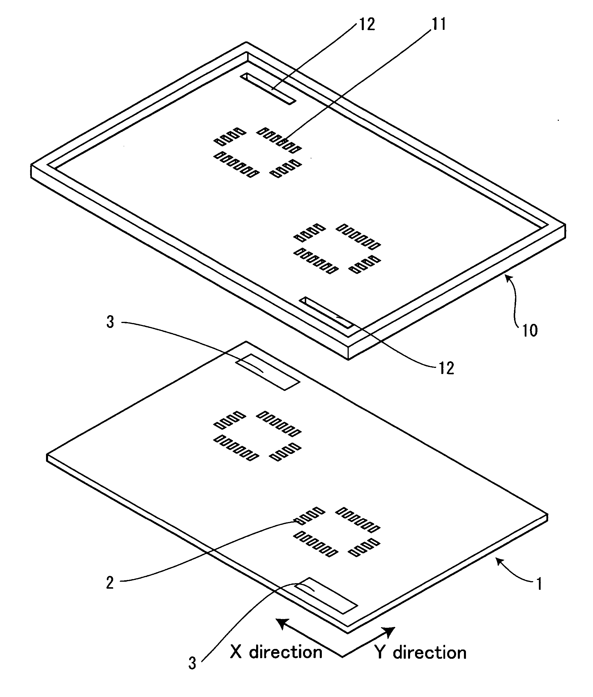
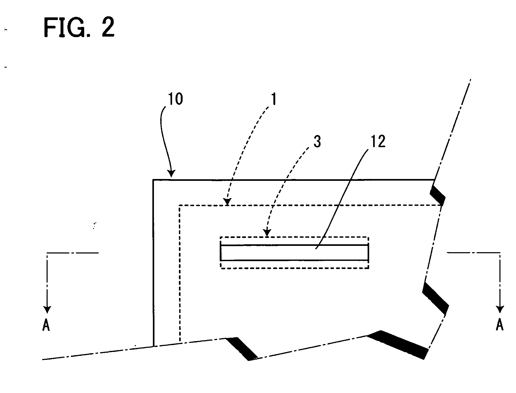
[0027]FIG. 1 to 6, show an embodiment of the present invention; FIG. 1 is a perspective view showing a circuit board on which cream solder of an embodiment 1 is printed, and a metal mask; FIG. 2 is a view showing a situation in which the circuit board and the metal mask are contacted each other, and the deviation angle is corrected; and FIG. 3 is a view showing a situation in which the cream solder is printed with the positioning lands and the positioning openings being deviated by an angle θ. FIG. 4 is a sectional view along the plane A-A of FIG. 2, and showing a process in which the cream solder is printed; (a) is ...


PUM

PropertyMeasurementUnit
lengthaaaaaaaaaa
lengthaaaaaaaaaa
lengthaaaaaaaaaa

Abstract

Rectangular positioning lands are formed on a circuit board, and rectangular positioning openings are formed in a metal mask. In addition, the positioning lands and positioning openings are formed such that their long side length becomes identical, and short side of the positioning opening becomes narrower than that of the positioning land. This enables to modify the deviation angle θ between the circuit board and the metal mask, and positional deviation in X and Y directions of the circuit board, during performing test printing, by modifying the position of the metal mask with respect to the circuit board, such that exposed excess parts, on which cream solder is not formed, are formed on the positioning lands, and the excess parts formed upper and lower sides of the cream solder mutually keep a constant spacing to become a same width.

Description

[0001] The present application is based on and claims priority of Japanese patent application No. 2005-045116 filed on Feb. 22, 2005, the entire contents of which are hereby incorporated by reference. BACKGROUND OF THE INVENTION [0002] 1. Field of the Invention [0003] The present invention relates to a cream solder printing metal mask, by which cream solder is printed from openings formed therein to land patterns of a circuit board by a squeegee sliding on the surface of the metal mask, especially, relates to a cream solder printing metal mask which is configured such that the land patterns and the openings are aligned, when the cream solder is printed, and its positioning method. [0004] 2. Description of the Related Art [0005] Conventionally, when a surface mounting electronic part is mounted on a circuit board, soldering is performed by printing cream solder on a land (conductive pattern) on the circuit board, positioning electrodes such as lead terminals of the electronic part on...

Claims


Application Information

Patent Timeline
Patent Type & Authority Applications(United States)
IPC IPC(8): B23K31/02B23K35/12B05C17/08
CPCB05B15/045B23K1/0016B23K2201/42H05K3/1225H05K3/3484H05K2201/09781H05K2203/166B05B12/20B23K2101/42H05K3/3485
Inventor KOYAMA, KIYOAKI
Owner ORION ELECTRIC CO LTD
Why Eureka
Try Eureka